Dual bit line precharge architecture and method for low power dynamic random access memory (DRAM) integrated circuit devices and devices incorporating embedded dram

a dynamic random access memory and integrated circuit technology, applied in the direction of information storage, static storage, digital storage, etc., can solve the problems of high power consumption in memory circuits, add extra cost to systems, and affect the overall operation of memory arrays, so as to reduce the power of dram memory arrays and therefore overall operating power, reduce current spikes and di/dt related noise effects, and reduce the effect of peak memory array curren

Active Publication Date: 2012-01-12
PROMOS TECH INC
View PDF13 Cites 6 Cited by
  • Summary
  • Abstract
  • Description
  • Claims
  • Application Information

AI Technical Summary

Benefits of technology

[0009]Power: The first embodiment of the present invention disclosed herein utilizes charge sharing techniques for non-VCC / 2 precharge designs to reduce DRAM memory array power and therefore overall operating power. This solves the problems with previous non-VCC / 2 bit line precharge approaches. The second embodiment of the present invention disclosed herein combines VSS and VCC precharged sub arrays on the same chip, which reduces current spikes and di / dt related noise effects.
[0010]Speed: Since in accordance with the present invention the peak memory array current is reduced, sensing and precharge control signals can be made faster with reduced concerns on internal voltage droop issues. This increases the overall speed of the DRAM.
[0011]Simplicity: The present invention may be conveniently implemented with existing CMOS circuit elements and any existing DRAM memory cell technologies.

Problems solved by technology

Nevertheless, for applications not utilizing battery power, power consumption can also be important.
Power consumption leading to heating problems can add extra expense to systems by way of requiring the use of cooling fans or larger heat sinks.
High power consumption in memory circuits may also require the system to operate at reduced clock frequencies.
The non VCC / 2 bit line precharge DRAM approaches do not have this power advantage and consume roughly double the memory array current or power as those utilizing VCC / 2 precharge.
The problem for DRAMs is since transistor threshold voltages cannot be reduced beyond a certain point and remain fixed in the 600 mV range due to fundamental physics of silicon, these reduced VCC voltages when divided in half do not allow for normal operation of complementary metal oxide semiconductor (CMOS) memory array control circuits.
In particular, the bit line sense amplifiers run out of operating margin and cannot function properly when the percentage level is near the transistor threshold voltage level.

Method used


Image

  • Dual bit line precharge architecture and method for low power dynamic random access memory (DRAM) integrated circuit devices and devices incorporating embedded dram
  • Dual bit line precharge architecture and method for low power dynamic random access memory (DRAM) integrated circuit devices and devices incorporating embedded dram
  • Dual bit line precharge architecture and method for low power dynamic random access memory (DRAM) integrated circuit devices and devices incorporating embedded dram

Examples


Embodiment Construction

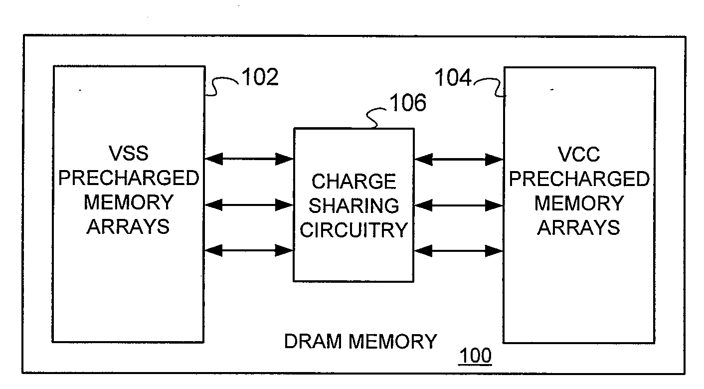
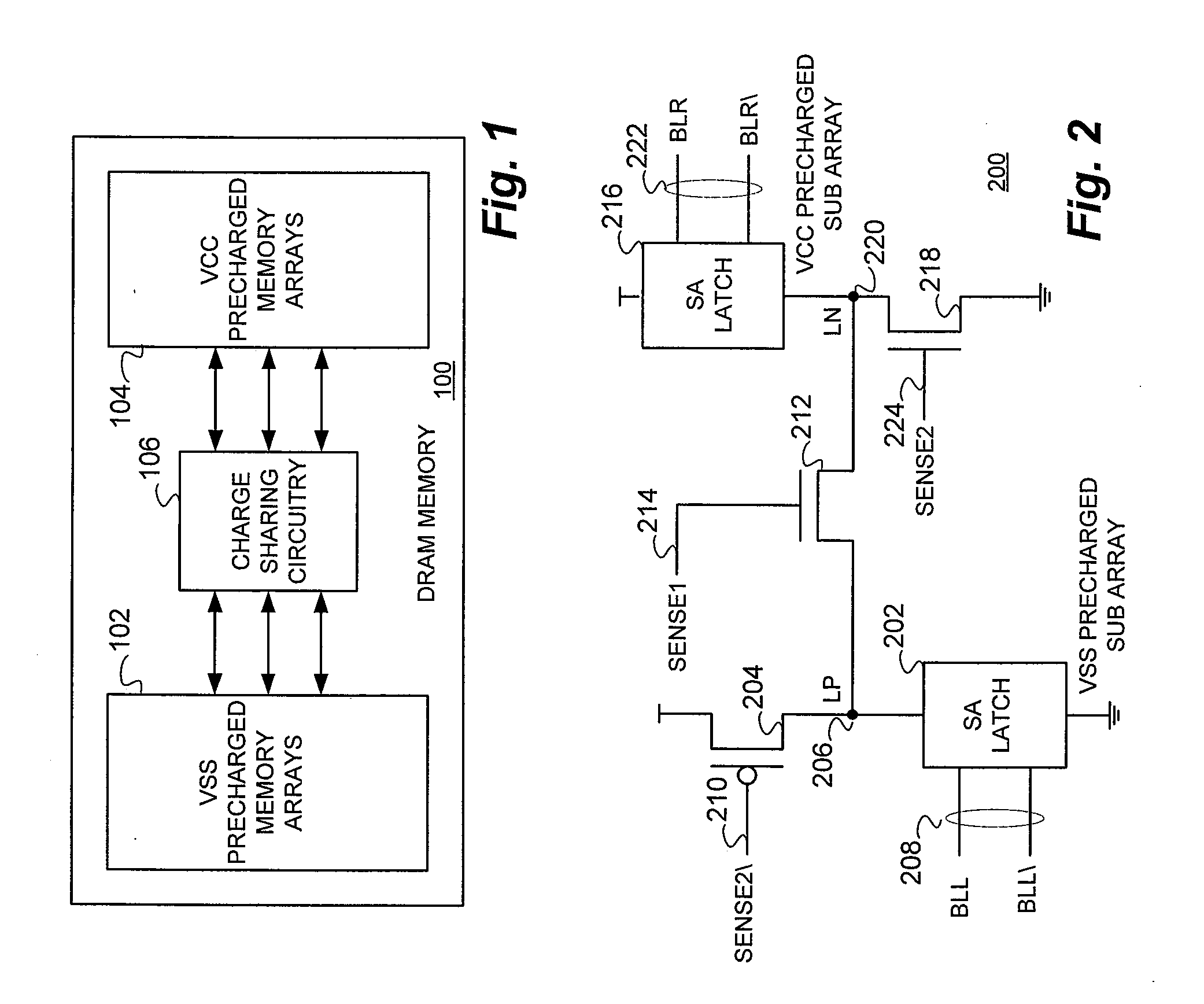
[0031]With reference now to FIG. 1, a representative block diagram of an integrated circuit device incorporating DRAM memory 100 in accordance with a particular embodiment of the present invention is shown. The DRAM memory 100 may be embedded DRAM forming a portion of an integrated circuit (IC) device or a dedicated, commodity DRAM IC. As illustrated the DRAM memory 100 comprises both a VSS bit line precharged memory array 102 and a VCC bit line precharged memory array 104 in conjunction with associated charge sharing circuitry 106 as will be more fully described hereinafter. In this particular embodiment of the present invention, through the combination of both VSS precharged memory sub arrays 102 and VCC precharged memory sub arrays 104 on the same DRAM memory 100 in conjunction with a unique charge sharing circuitry 106, memory array power requirements can be reduced to half of that utilized in conventional VCC / 2 precharged memories.

[0032]As disclosed herein, memory array 102 rep...


PUM


Abstract

A dual bit line precharge architecture and method for low power DRAM which provides the low operating voltage of a non-half supply voltage (VCC/2) precharge with the low memory array current consumption and low memory array noise spike of VCC/2 precharge techniques. The architecture and technique of the present invention provides both reference voltage (VSS) precharged sub arrays and VCC precharged sub arrays on the same DRAM memory either with or without the novel charge sharing or charge recycling circuitry between these two different sub arrays as disclosed herein.

Description

CROSS REFERENCE TO RELATED PATENT APPLICATIONS[0001]The present invention is related to United States patent application Ser. No. [UMI-506 DIV] filed on even date herewith for DUAL BIT LINE PRECHARGE ARCHITECTURE AND METHOD FOR LOW POWER DYNAMIC RANDOM ACCESS MEMORY (DRAM) INTEGRATED CIRCUIT DEVICES AND DEVICES INCORPORATING EMBEDDED DRAM and assigned to ProMOS Technologies PTE.LTD., the disclosure of which is herein specifically incorporated by this reference.BACKGROUND OF THE INVENTION[0002]The present invention relates, in general, to the field of dynamic random access memory (DRAM) integrated circuit (IC) devices and devices incorporating embedded DRAM. More particularly, the present invention relates to a dual bit line precharge architecture and method for low power DRAM.[0003]Lower power consumption is a major design goal for today's integrated circuit memories. Many applications for memory devices are mobile and the ability to provide extended battery life can be a key market...

Claims


Application Information

Patent Timeline
Patent Type & Authority Applications(United States)
IPC IPC(8): G11C7/00
CPCG11C11/4091G11C11/4097G11C11/4094
Inventor PARRIS, MICHAEL C.HARDEE, KIM C.
Owner PROMOS TECH INC
Why Eureka
Try Eureka