Programmable-resistance memory cell

a memory cell and resistance technology, applied in the direction of bulk negative resistance effect devices, electrical apparatus, semiconductor devices, etc., can solve the problems of time-consuming conditioning process, inability to control the conductor path, and required conductors, and achieve the effect of low operating power

Inactive Publication Date: 2010-05-25
GLOBALFOUNDRIES U S INC
View PDF7 Cites 14 Cited by
  • Summary
  • Abstract
  • Description
  • Claims
  • Application Information

AI Technical Summary

Benefits of technology

[0009]According to an embodiment of a first aspect of the present invention, there is provided a memory cell comprising: at least a source electrode formed on a substrate; at least a drain electrode formed on the substrate; at least a coupling layer between the source electrode and the drain electrode, and at least a gate electrode formed on the substrate, wherein: the coupling layer comprises a transition-metal oxide exhibiting a filling-controlled metal-insulator transition property; the gate electrode comprises an oxygen-ion conductor layer, and the gate electrode is arranged relative to the coupling layer such that application of an electrical signal to the gate electrode causes alteration of an oxygen vacancy concentration in the coupling layer. In an embodiment of the present invention, the electrical signal that is applied to the gate electrode causes oxygen vacancies to migrate into the coupling layer from the oxygen-ion conductor layer. This changes the formal oxidation state of the transition-metal ion in the transition-metal oxide and concomitantly the filling of the transition metal band. Thus, the coupling layer is transformed from having substantially insulating properties to a conductor and vice versa when an electrical signal is applied to the gate electrode. Thus, in an embodiment of the present invention, the resistance of the coupling layer is reversibly switchable between at least two different and persistent resistance states by the application of the electrical signal to the gate electrode. More particularly, resistance switching may be achieved in an embodiment of the present invention without initiation of a conditioning process as for previously-proposed devices and so does not suffer from the above-discussed drawbacks associated to the conditioning process. Furthermore, the resistance state of the coupling layer that is set by the application of an electrical signal to the gate electrode persists until the application of an electrical signal to the gate electrode again, i.e. the electrical signal need not be applied continuously to the gate electrode for a set and desired resistance set to persist and so an embodiment of the present invention offers the advantage of lower operating power than previously-proposed devices. A further advantage associated to an embodiment of the present invention is that multi-level, multi-bit, storage per cell is possible.
[0010]Preferably, the oxygen-ion conductor layer comprises a material exhibiting an oxygen vacancy mobility of at least 10−9 cm2 / Vs. Selection of the material of the oxygen-ion conductor layer to exhibit an oxygen vacancy mobility that is high, i.e. at least 10−9 cm2 / Vs, is reflected in the reduced time for oxygen vacancies to migrate from the oxygen-ion conductor layer into the coupling layer, and, therefore, in the switching of the resistance state of the coupling layer from an off state, when it is substantially insulating, to an on state in which it conducts current, or vice versa, when an electrical signal is applied to the gate electrode.
[0011]Desirably, the arrangement of the gate electrode relative to the coupling layer is such that the oxygen-ion conductor layer is formed on the coupling layer. In this case, since the oxygen-ion conductor layer is formed directly on the coupling layer, the migration of oxygen vacancies into the coupling layer is aided.

Problems solved by technology

Some of the drawbacks of the above-described devices are associated with the conditioning process.
This is because, not only is the conditioning process time-consuming, it is required per cell incorporated in such a device.
Furthermore, the confined conductive region that is generated by the conditioning process occurs at an arbitrary position in the dielectric material, i.e., the position of the conducting path is not controllable by well-defined process parameters.

Method used


Image

  • Programmable-resistance memory cell
  • Programmable-resistance memory cell
  • Programmable-resistance memory cell

Examples


Embodiment Construction

[0022]Within the description, the same reference numerals or signs have been used to denote the same parts or the like.

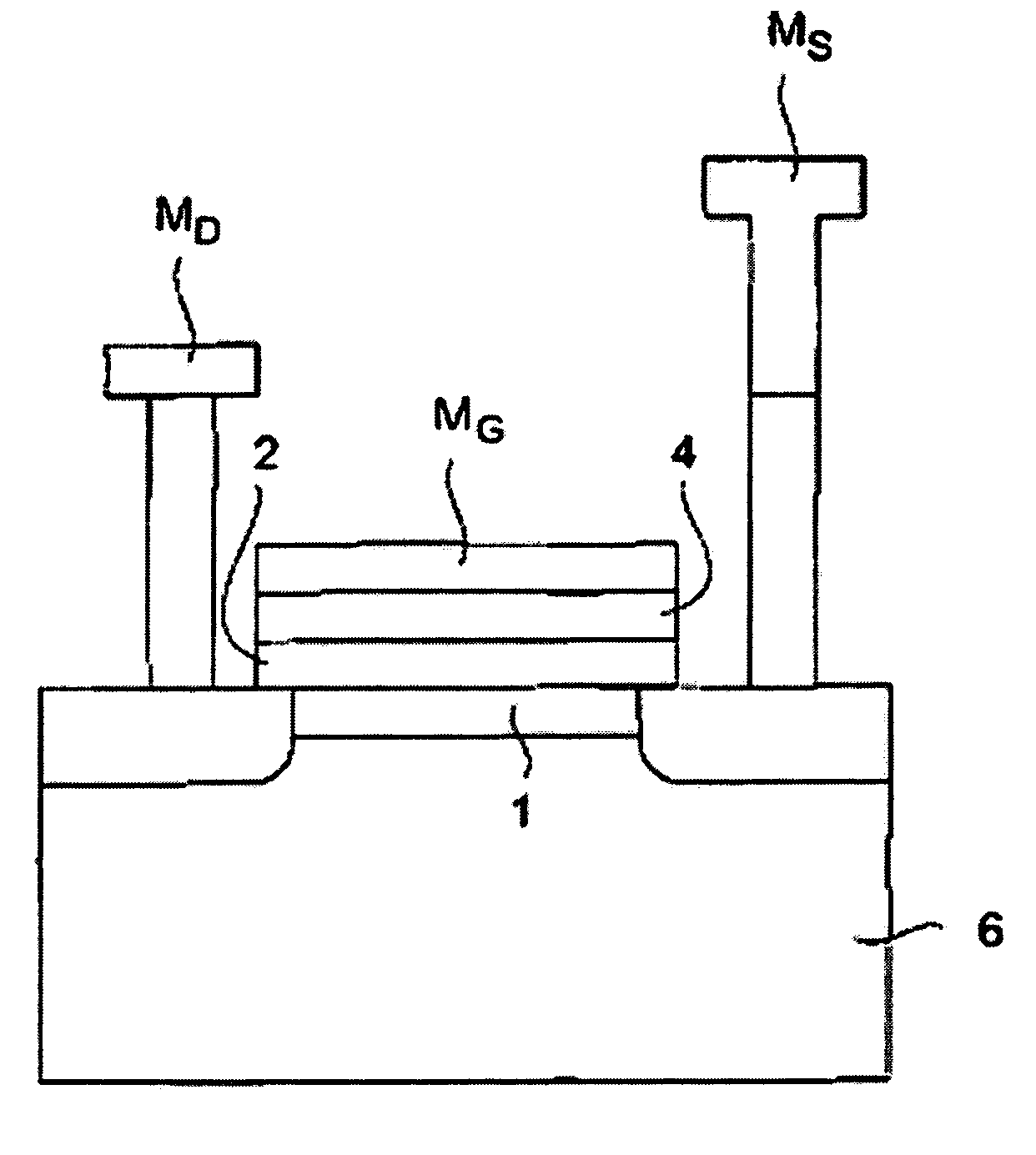
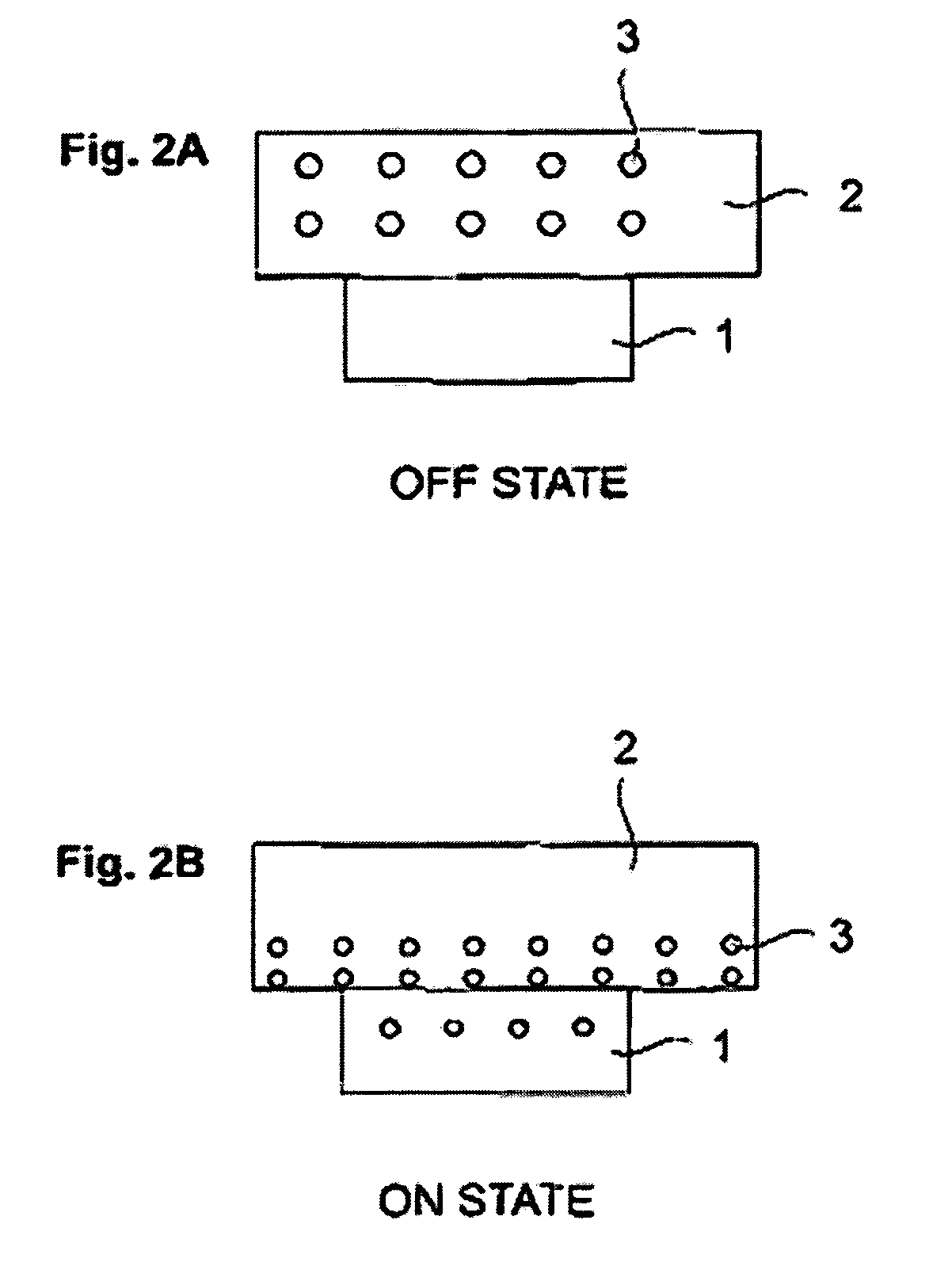
[0023]Reference is now made to FIG. 1, which schematically illustrates an embodiment of the present invention. As can be seen from FIG. 1, in an embodiment of the present invention, there is provided a memory cell 10 with three terminals: a source electrode MS, a drain electrode MD and a gate electrode MG all of which are formed on a substrate 6. The substrate 6 may, for example, pertain to CMOS technology and be made of silicon-dioxide (SiO2). The source electrode MS and the drain electrode MD, which are shown as being arranged laterally relative to each other, are connected by a coupling layer 1, which is chosen to comprise a transition-metal oxide exhibiting a filling-controlled metal-insulator transition property. The gate electrode MG is formed so as to comprise an oxygen-ion conductor layer 2. By oxygen-ion conductor layer, it is meant that such a layer compri...


PUM


Abstract

A memory cell (10) comprising at least a source electrode (MS) formed on a substrate (6); at least a drain electrode (MD) formed on the substrate (6); at least a coupling layer (1) formed between the source electrode (MS) and the drain electrode (MD), and at least a gate electrode (MG) formed on the substrate (6), wherein the coupling layer (1) comprises a transition-metal oxide exhibiting a filling-controlled metal-insulator transition property; the gate electrode (MG) comprises an oxygen ion conductor layer (2), and the gate electrode (MG) is arranged relative to the coupling layer (1) such that application of an electrical signal to the gate electrode (MG) causes alteration of the oxygen vacancy (3) concentration in the coupling layer (1).

Description

FIELD OF THE INVENTION[0001]The present invention relates to a programmable-resistance memory cell, a method of fabrication therefor and a non-volatile memory device incorporating such a memory cell.BACKGROUND OF THE INVENTION[0002]For memory devices and for numerous other applications, bi-stable devices or circuits are used. For example, for storing one bit of information in a memory, a bi-stable device can be used which is switchable between at least two different and persistent states. When writing a logical “1” into the device, it is driven into one of the two persistent states and when writing a logical “0”, or erasing the logical “1”, the device is driven into the other of the two different states. Each of the states persists until a next step of writing information into the device or erasing information in the device proceeds.[0003]Flash erasable programmable read only memory (FEPROM, also referred to as flash memory) is used in semiconductor devices and provides for rapid bl...

Claims


Application Information

Patent Timeline
Patent Type & Authority Patents(United States)
IPC IPC(8): H01L45/00
CPCH01L45/08H01L45/147H01L45/1266H01L45/1206H10N70/253H10N70/24H10N70/8416H10N70/8836
Inventor KARG, SIEGFRIED F.MEIJER, GERHARD INGMAR
Owner GLOBALFOUNDRIES U S INC
Why Eureka
Try Eureka