

Method for designing semiconductor integrated circuit and automatic designing device
- Summary
- Abstract
- Description
- Claims
- Application Information
AI Technical Summary
Benefits of technology
Problems solved by technology
Method used
Image

Examples
Embodiment Construction
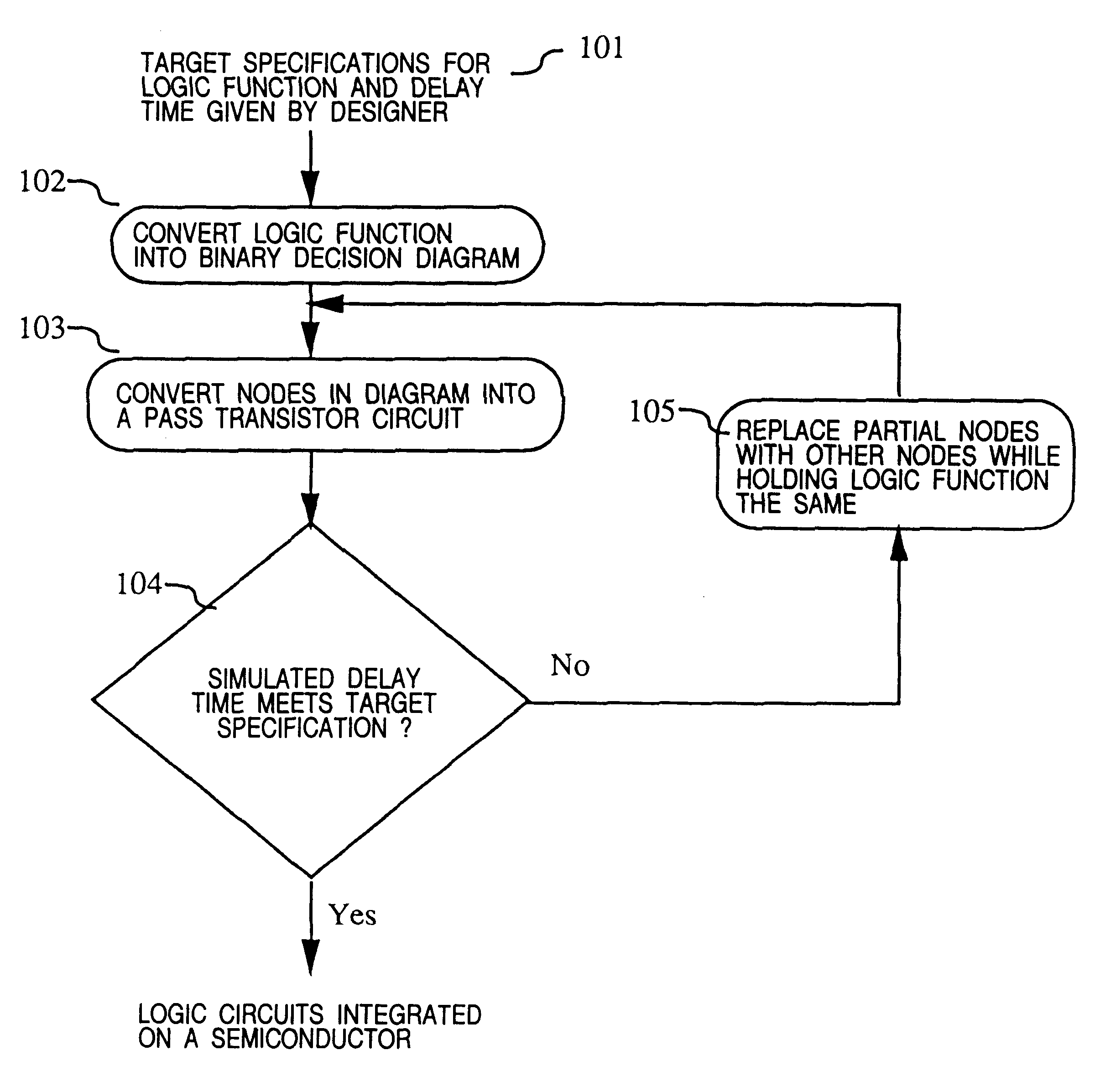
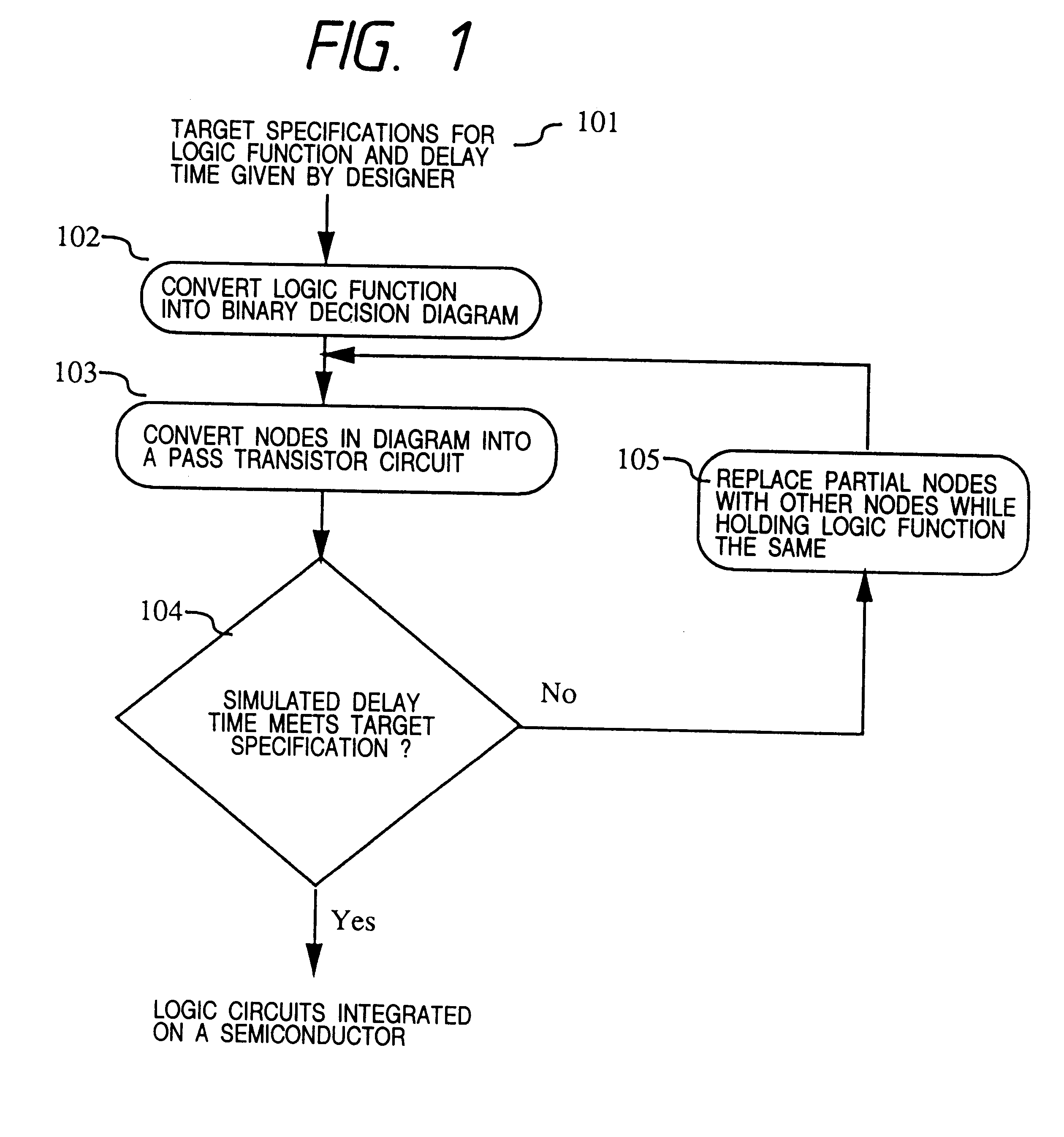
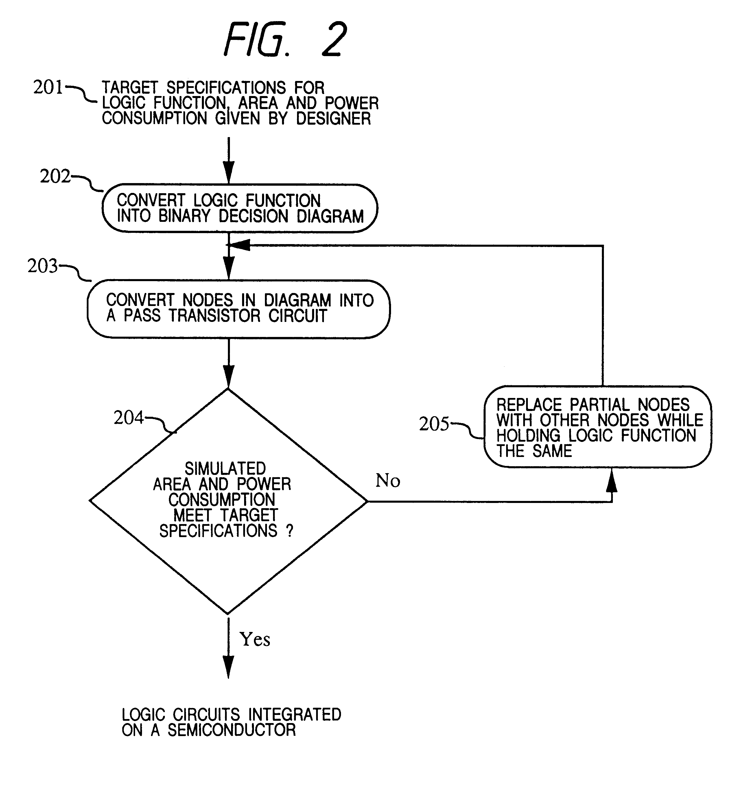
Referring to FIG. 1, there is shown a logic circuit designing method for a semiconductor integrated circuit according to an embodiment of the present invention.
The design method according to this embodiment is a method of designing a logic circuit to be integrated on a semiconductor, as implemented by using an automatic designing device (1101) shown in FIG. 11, which comprises a central processing unit (CPU) (not shown), a memory device (including a main memory, hard disk storage, etc.) (not shown) and a man-machine interface devices (including a keyboard, display monitor, touch-sensitive panel, etc.) (not shown). The method has feature that a program held in the memory device (not shown) of the automatic designing device (1101) executes the following steps and automatically designs a logic circuit to be integrated on semiconductor.
Step 101 in FIG. 1: In this step 101, (a) a logic function for determining logic relationship between logic inputs and logic outputs as shown by 301 in F...
PUM
 Abstract
Description
Claims
Application Information