
Housing for piezoelectric transformer device

a piezoelectric transformer and housing technology, applied in the direction of printed circuit assembling, printed circuit manufacturing, generators/motors, etc., can solve the problems of low productivity, low productivity, and deterioration of output characteristics of piezoelectric transformers, and achieve the effect of convenient mounting and facilitating the housing process

Inactive Publication Date: 2001-07-17
TAIHEIYO CEMENT CORP
View PDF8 Cites 10 Cited by
  • Summary
  • Abstract
  • Description
  • Claims
  • Application Information

AI Technical Summary

Benefits of technology

It is an object of the present invention to provide a housing that facilitates a housing process for a piezoelectric transformer device and can be easily mounted on a circuit board.
Note that the formation of the opening 7 described in FIGS. 11 and 12 may be omitted to decrease the number of steps of designing a mold for the housing 1 and the manufacturing cost. Obviously, however, the opening 7 is preferably formed to facilitate a check on the connection state between the lead electrodes and the outer electrodes of the piezoelectric device 106 while the piezoelectric device 106 is housed in the housing 1 and to allow easy connection between the lead electrodes and the outer electrodes of the piezoelectric device 106 with a conductive adhesive or by soldering, as needed, through the opening 7 so as to improve the reliability of the piezoelectric transformer.

Problems solved by technology

If this vibration is inhibited when the device is mounted on the circuit board, the output characteristics of the piezoelectric transformer deteriorate.
When the piezoelectric device is to be housed in the above general housing, a large number of steps are required, ranging from the step of housing the piezoelectric device in the housing to the step of connecting the lead wires on the circuit board, resulting in low productivity.
When terminals to which the lead wires of the piezoelectric device are connected are to be formed on the housing, and the housing is to be mounted on the circuit board through the terminals, a large number of steps are required in mounting the housing, resulting in low productivity.
If, therefore, an external shock or vibration acts on this housing, the electric connection between the piezoelectric device and the terminals may be broken, resulting in instantaneously disconnection.

Method used


Image

  • Housing for piezoelectric transformer device
  • Housing for piezoelectric transformer device
  • Housing for piezoelectric transformer device

Examples


second embodiment

The second embodiment of the present invention will be described with reference to FIGS. 28 to 33.

The outer shape of a housing 21 will be described first. FIG. 28 is a perspective view showing the housing according to the second embodiment of the present invention. FIG. 29 is a plan view of the housing in FIG. 28.

In the housing 21 shown in FIGS. 28 and 29, lead electrodes 24 and 25, mount terminals 24a and 25a, and amount terminal 26 respectively have the same structures and functions as those of the lead electrodes 4 and 5, the mount terminals 4a and 5a, and the mount terminal 6 in the first embodiment described above, and hence a description thereof will be omitted.

The structural characteristics of the housing 21 according to this embodiment will be described next. FIG. 30 is a bottom view of the housing in FIG. 28. FIG. 31 is a sectional view taken along a line XI--XI in FIG. 29. FIG. 32 is a sectional view taken along a line XII--XII in FIG. 30.

As shown in FIGS. 30 to 32, in thi...


PUM


Abstract

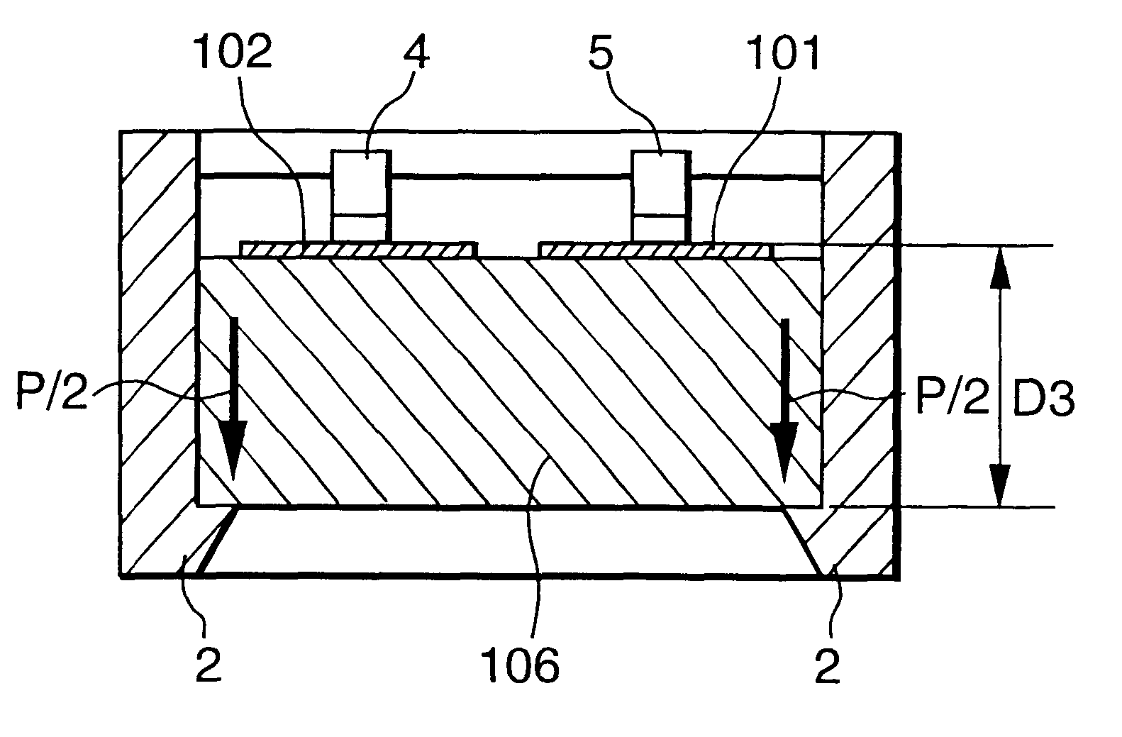
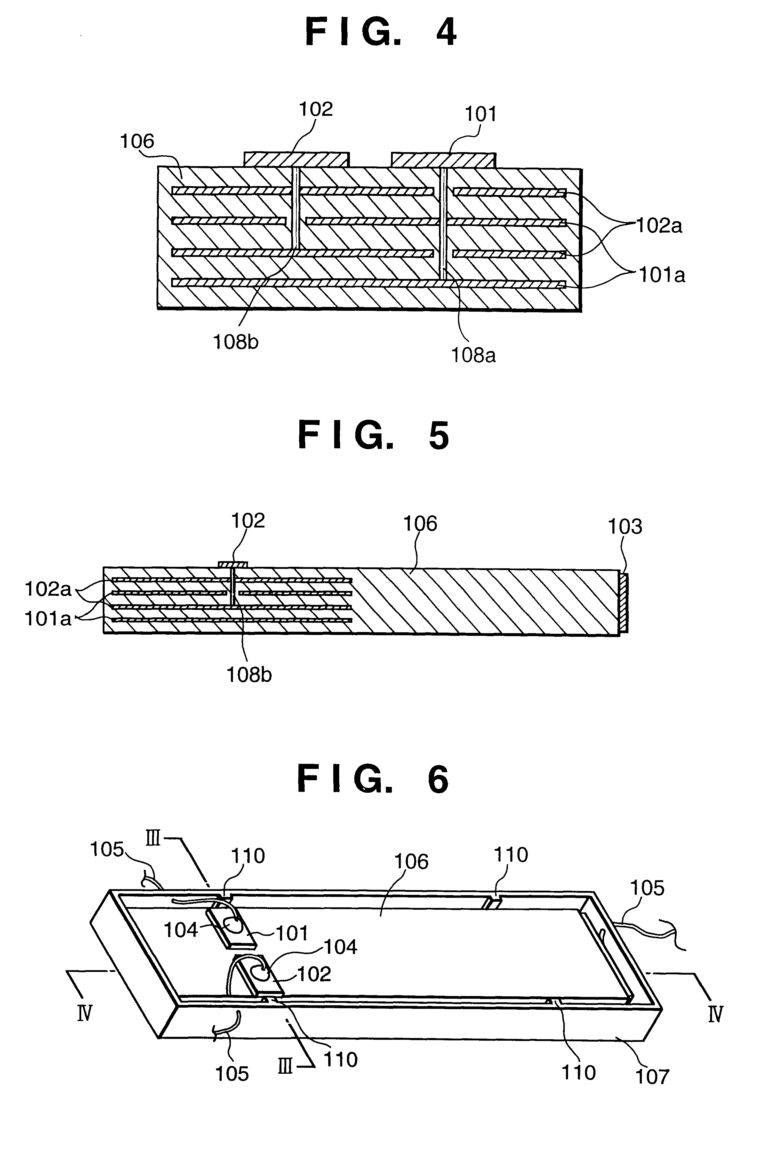
Mount terminals (4a, 5a, 6) are formed on end faces of a housing (1). These mount terminals serve to mount the housing (1) on a circuit board and also serves as lead electrodes for the outer and output electrodes of a piezoelectric device to be housed in the case. The piezoelectric device is fixed in the housing (1) by using the lead electrodes (4, 5) integrally formed with mount terminals (4a, 5a) and projections (2, 3).

Description

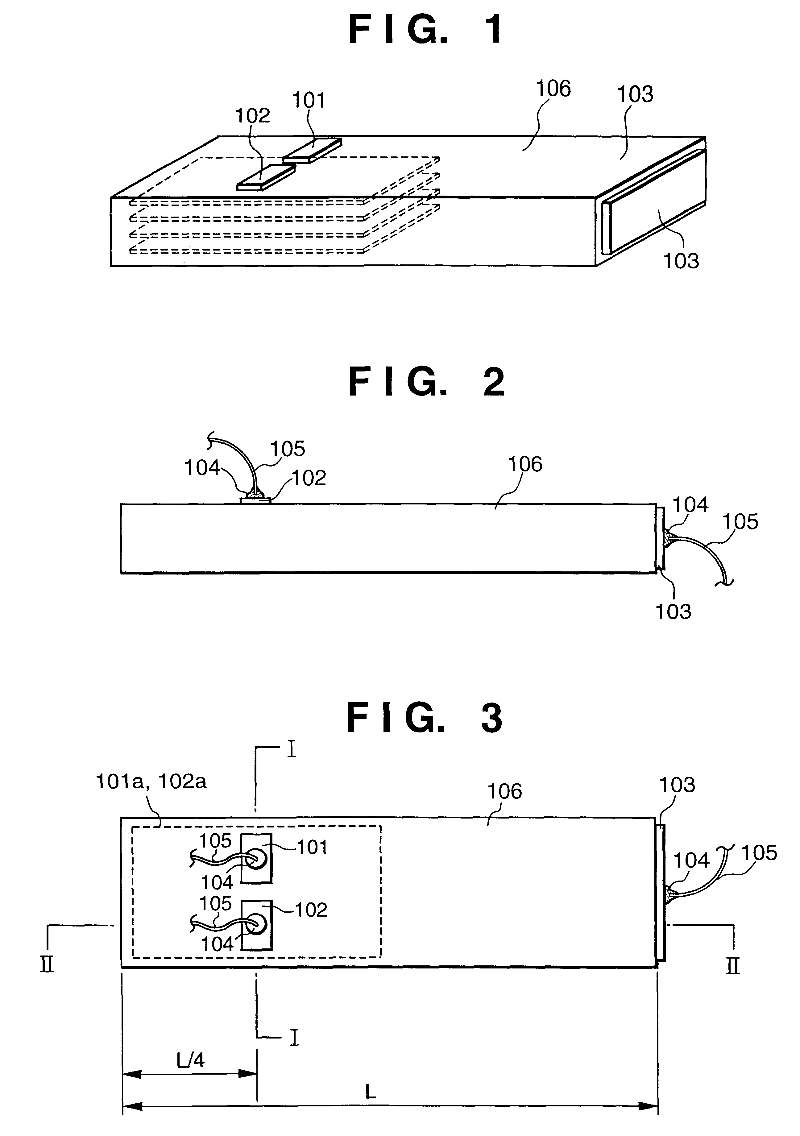
The present invention relates to a housing for a piezoelectric transformer device, e.g., a housing for mounting a Rosen piezoelectric transformer on a circuit board.Recently, liquid crystal display panels have been widely used as display units in notebook personal computers which are easy to carry. Such a liquid crystal display panel incorporates a cold-cathode fluorescent lamp serving as a backlight for backlighting the panel. In order to light this cold-cathode fluorescent lamp, a high voltage of about 1 kV or more is required. To maintain emission of light, a voltage of about several hundred volts must be applied.In such notebook personal computers and similar products, owing to their characteristics, the demand for compact inverters for backlights is high. In order to meet this demand, piezoelectric transformers are used as inverter components.As such a piezoelectric transformer, the piezoelectric transformer device (to be referred to as the piezoelectric device hereinafter) hav...

Claims


Application Information

Patent Timeline
Patent Type & Authority Patents(United States)
IPC IPC(8): H01L41/00H01L41/107H01L41/053H05K3/30H01L23/08H10N30/40H10N30/88
CPCH01L41/053H01L41/107H05K3/301H10N30/88H10N30/40
Inventor ISHIKAWA, KATSUYUKIFUJIMURA, TAKESHITOYAMA, MASAAKIUESAWA, KATSUMI
Owner TAIHEIYO CEMENT CORP
Learn More