Photoconductive switch
- Summary
- Abstract
- Description
- Claims
- Application Information
AI Technical Summary
Problems solved by technology
Method used
Image

Examples
Embodiment Construction
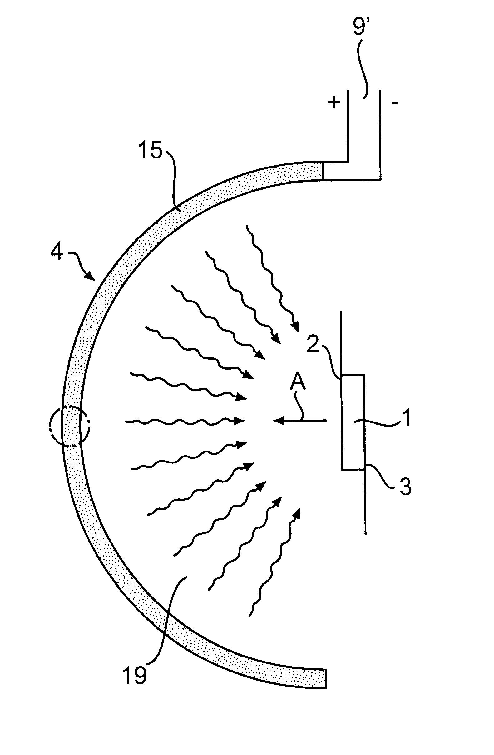
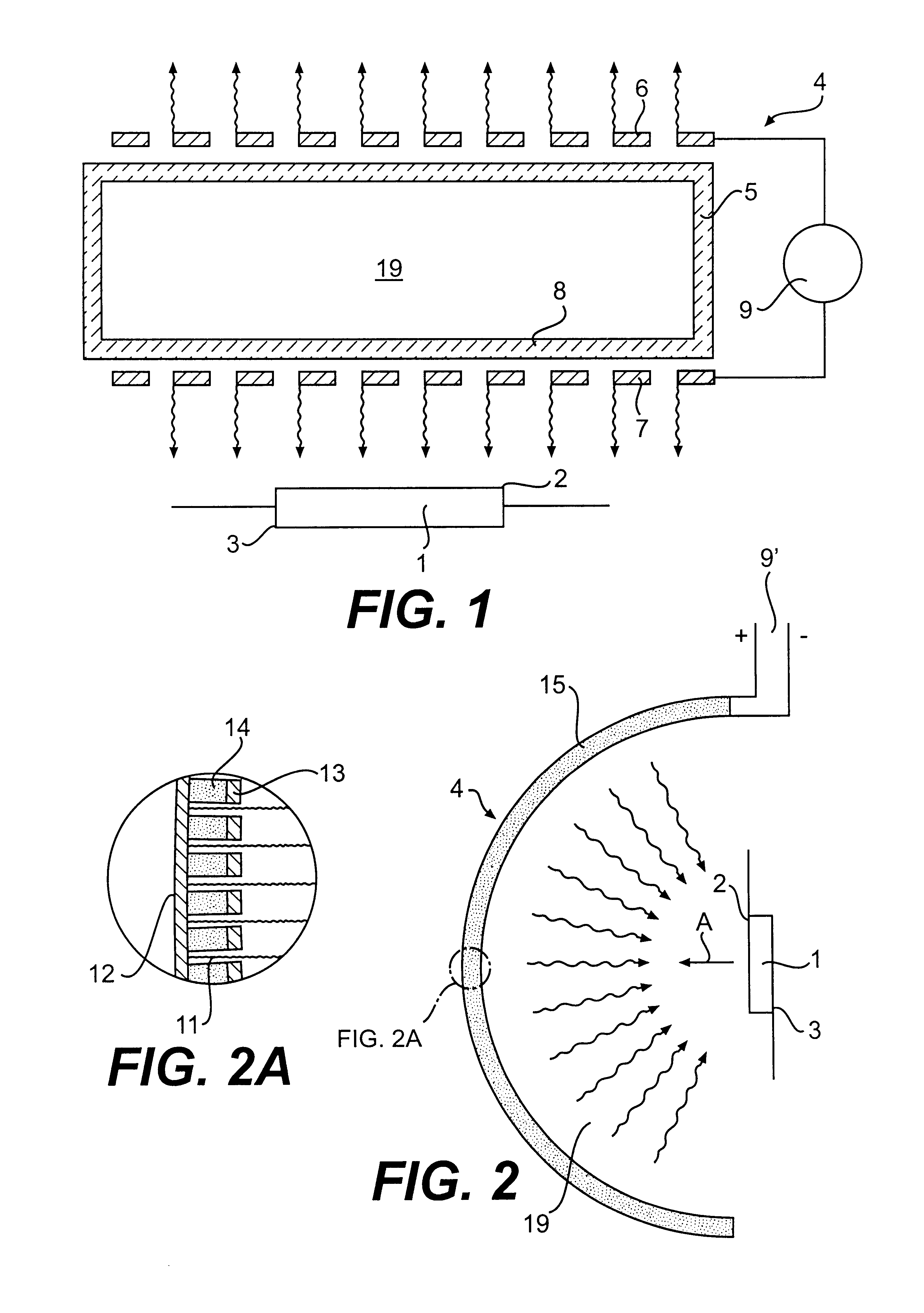
A switch according to a first preferred embodiment of the invention is very schematically shown in FIG. 1, and this photoconductive switch has a first layer 1, which in this case is made of intrinsic diamond, and two contact layers 2, 3 connectable to different potentials for applying a voltage across the first layer. Accordingly, the two contact layers are adapted to be connected to for example an electric circuit of an apparatus for controlling a power network.
The switch also comprises an irradiation source 4 which has a casing 5 hermetically enclosing a gas or gas mixture having gas atoms able to form unstable electronically excited dimers when such a voltage is applied over a gap in said volume that free electrons are created an accelerated to come into collision with said gas atoms for excitation thereof. Two electrodes 6, 7 of a means for generating said voltage for creation of free electrons in the volume 19 of the casing are arranged outside said casing on opposite sides the...
PUM
 Abstract
Description
Claims
Application Information
 - R&D Engineer
- R&D Manager
- IP Professional
- Industry Leading Data Capabilities
- Powerful AI technology
- Patent DNA Extraction
Browse by: Latest US Patents, China's latest patents, Technical Efficacy Thesaurus, Application Domain, Technology Topic.
© 2024 PatSnap. All rights reserved.Legal|Privacy policy|Modern Slavery Act Transparency Statement|Sitemap