Structure design of tunnel junction in Perovskite/silicon heterojunction lamination solar battery

A silicon heterojunction and stacked solar technology, applied in the field of solar cells, can solve problems such as the influence of open circuit voltage, achieve the effects of hole recombination improvement, tunneling probability improvement, and avoiding a large amount of accumulation

Inactive Publication Date: 2018-01-09
NANKAI UNIV +1
View PDF3 Cites 31 Cited by
  • Summary
  • Abstract
  • Description
  • Claims
  • Application Information

AI Technical Summary

Problems solved by technology

[0004] The purpose of the present invention is to solve the problem of the influence of the reverse tunneling junction on the open circuit voltage of the laminated solar cell, and to provide a structural design of the tunneling junction in the perovskite / silicon heterojunction laminated solar cell. A narrow band gap, high doping concentration, and high transmittance material is introduced into the battery as the TRL (Tunnel Recombination Layer) of the perovskite / silicon heterojunction stack solar cell

Method used


Image

  • Structure design of tunnel junction in Perovskite/silicon heterojunction lamination solar battery
  • Structure design of tunnel junction in Perovskite/silicon heterojunction lamination solar battery

Examples


Embodiment 1

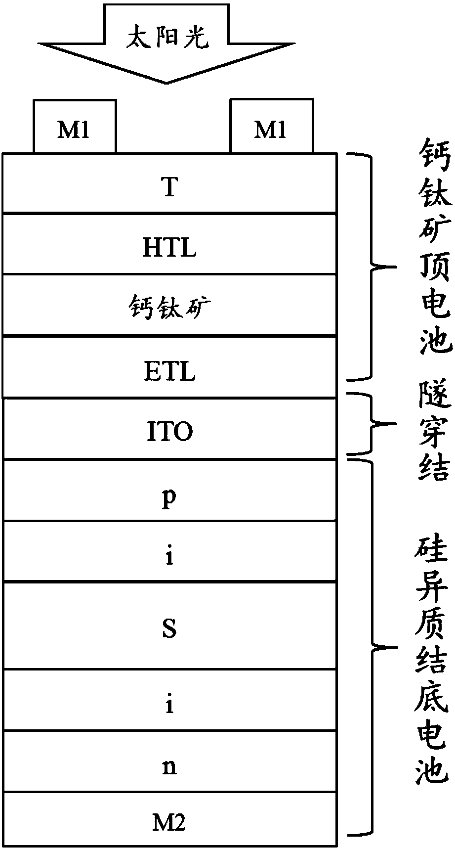
[0019] This embodiment is a structure of a traditional perovskite / silicon heterojunction stacked solar cell, such as figure 1 As shown, it includes from top to bottom: metal grid line electrode M1, transparent electrode T, perovskite top cell hole transport material HTL, perovskite absorption layer, top cell electron transport material ETL, tunnel junction ITO, silicon The hole selection layer p of the heterojunction bottom cell, the passivation layer i, the substrate S, the electron selection layer n and the metal back electrode M2.

[0020] Wherein the crystalline silicon layer S is n-type polished single crystal silicon.

[0021] The silicon heterojunction solar cell of this embodiment is prepared by the following method:

[0022] 1. Place the polished Cz silicon wafer substrate with N-type crystal orientation in a PECVD system with high vacuum, and deposit a layer of intrinsic amorphous silicon passivation layer i on the front and back surfaces of the silicon wafer.

[...

Embodiment 2

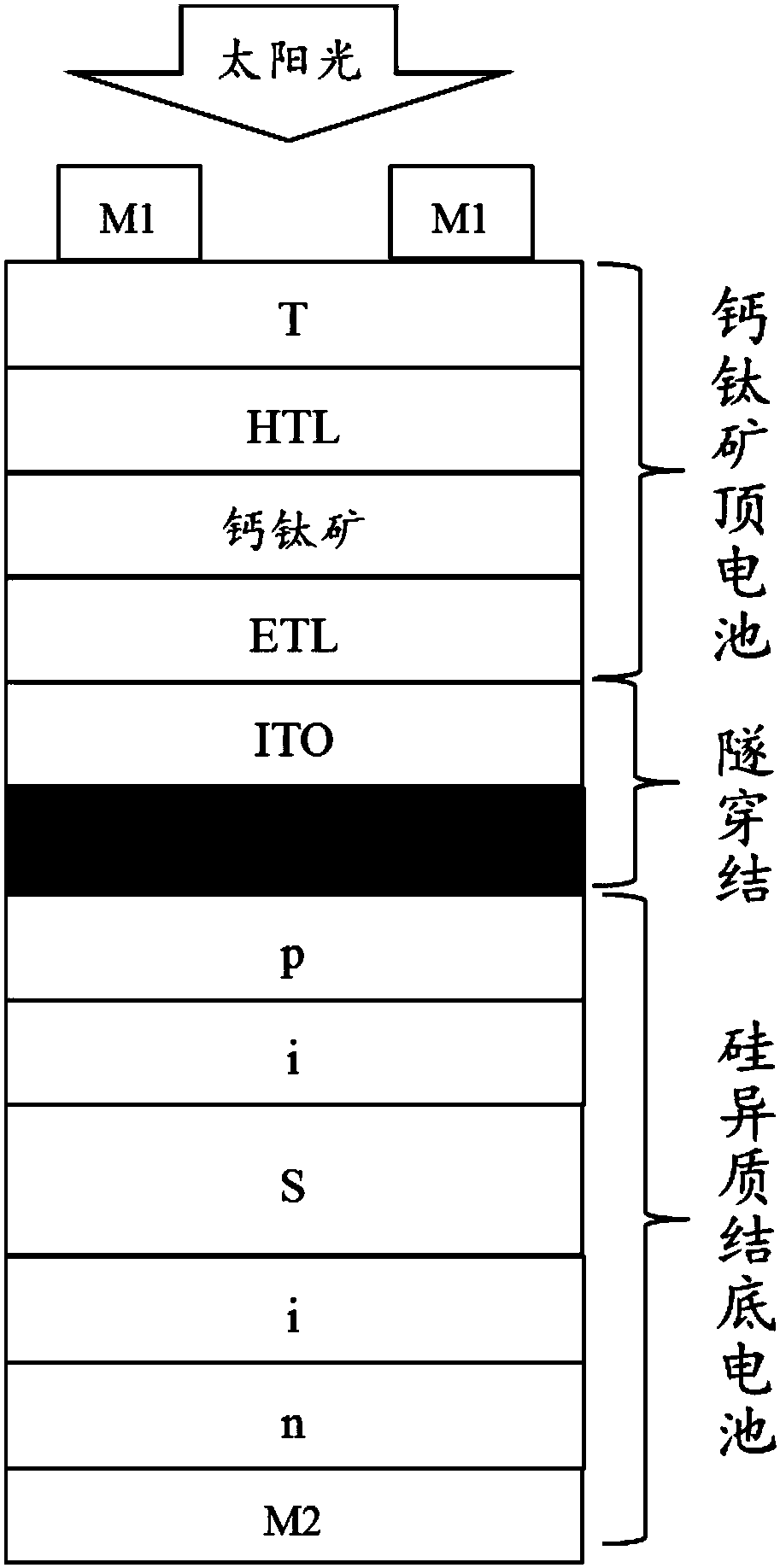
[0030] This embodiment is a structure of a perovskite / silicon heterojunction stacked solar cell provided by the present invention, such as figure 2 As shown, it includes from top to bottom: metal grid line electrode M1, transparent electrode T, perovskite top cell hole transport material HTL, perovskite absorption layer, top cell electron transport material ETL, tunnel junction ITO+TRL , silicon heterojunction bottom cell hole selection layer p, passivation layer i, substrate S, passivation layer i, electron selection layer n and metal back electrode M2.

[0031] The TRL is n-μc-Si:H, the thickness is 10nm, the gap is 1.7eV, the conductivity is 2s / cm, and the long-wavelength transmittance is 81%.

[0032] The crystalline silicon layer S is n-type polished single crystal silicon.

[0033] The silicon heterojunction solar cell of this embodiment is prepared by the following method:

[0034] 1. Place the polished Cz silicon wafer substrate with N-type crystal orientation in a...

Embodiment 3

[0043] This embodiment is a structure of a perovskite / silicon heterojunction stacked solar cell provided by the present invention, such as figure 2 Shown, concrete structure is with embodiment 2, is omitted here.

[0044] Where TRL is p-μc-Si:H / n-μc-Si:H, and the thicknesses are 0.5nm and 10nm, respectively.

[0045] The crystalline silicon layer S is n-type polished single crystal silicon.

[0046] The subsequent process of the silicon heterojunction solar cell in this embodiment is the same as that in Embodiment 2, which is omitted here.

[0047] The p / n-μc Si:H is applied to the preparation process of the perovskite / silicon heterojunction tandem solar cell, and the opening voltage of the perovskite / silicon heterojunction solar cell is 1.71V.


PUM


Abstract

The invention provides a structure design of tunnel junction in Perovskite / silicon heterojunction lamination solar battery, which relates to the field of solar batteries. A tunneling composite layer TRL with narrow band gap and high doping concentration is added at the junction of the top and bottom part of a lamination battery, and the quite small energy level difference between the conduction band and the valence band can effectively strengthen the carrier recombination at the tunneling junction. The gradient band order at the bottom battery p layer and the tunneling junction can effectivelyenhance the cavity draw-off of the bottom battery and the tunneling junction, and thereby a large amount of charge accumulation among the tunneling junction interfaces can be prevented. After the adding of the TRL having high doping concentration, the defect density of states at the tunneling junction is increased. The electronic cavity assists tunneling through defects, and the probability of recombination and tunneling can be increased. With the adoption of the heterojunction, the spectrum response of the bottom battery can be effectively enhanced, and the opening and pressing loss can be reduced. The preparation method is simple and easy to carry out.

Description

technical field [0001] The invention belongs to the technical field of solar cells, and in particular relates to a structure design of a tunnel junction in a perovskite / silicon heterojunction laminated solar cell. Background technique [0002] Solar photovoltaic power generation has developed rapidly due to its advantages of safety, reliability, less geographical constraints, and easy integration with buildings. In order to enable it to be applied on a large scale, reducing production costs and improving the photoelectric conversion efficiency of solar cells are two key points. The energy distribution of the sunlight spectrum is very wide, and semiconductor materials can only absorb photons whose energy is higher than its forbidden band width value, so broadening the solar absorption range of the battery and enhancing the absorption and utilization of sunlight are the key to improving the solar battery. effective approach to photoelectric conversion efficiency. Among many ...

Claims


Application Information

Patent Timeline
Patent Type & Authority Applications(China)
IPC IPC(8): H01L31/0725H01L31/074H01L51/42
CPCY02E10/549Y02P70/50
Inventor 张晓丹姚鑫朱世杰郑翠翠任千尚李盛喆魏长春丁毅任慧志黄茜李宝璋赵颖
Owner NANKAI UNIV
Why Eureka
Try Eureka