

Process system
a technology of process system and process system, applied in the field of process system, can solve the problems of increasing the number of coating and developing process system, the inability to dynamically expand or reduce the system, and the inability to dynamically expand the system for example two or three times
- Summary
- Abstract
- Description
- Claims
- Application Information
AI Technical Summary
Benefits of technology
Problems solved by technology
Method used
Image

Examples
first embodiment
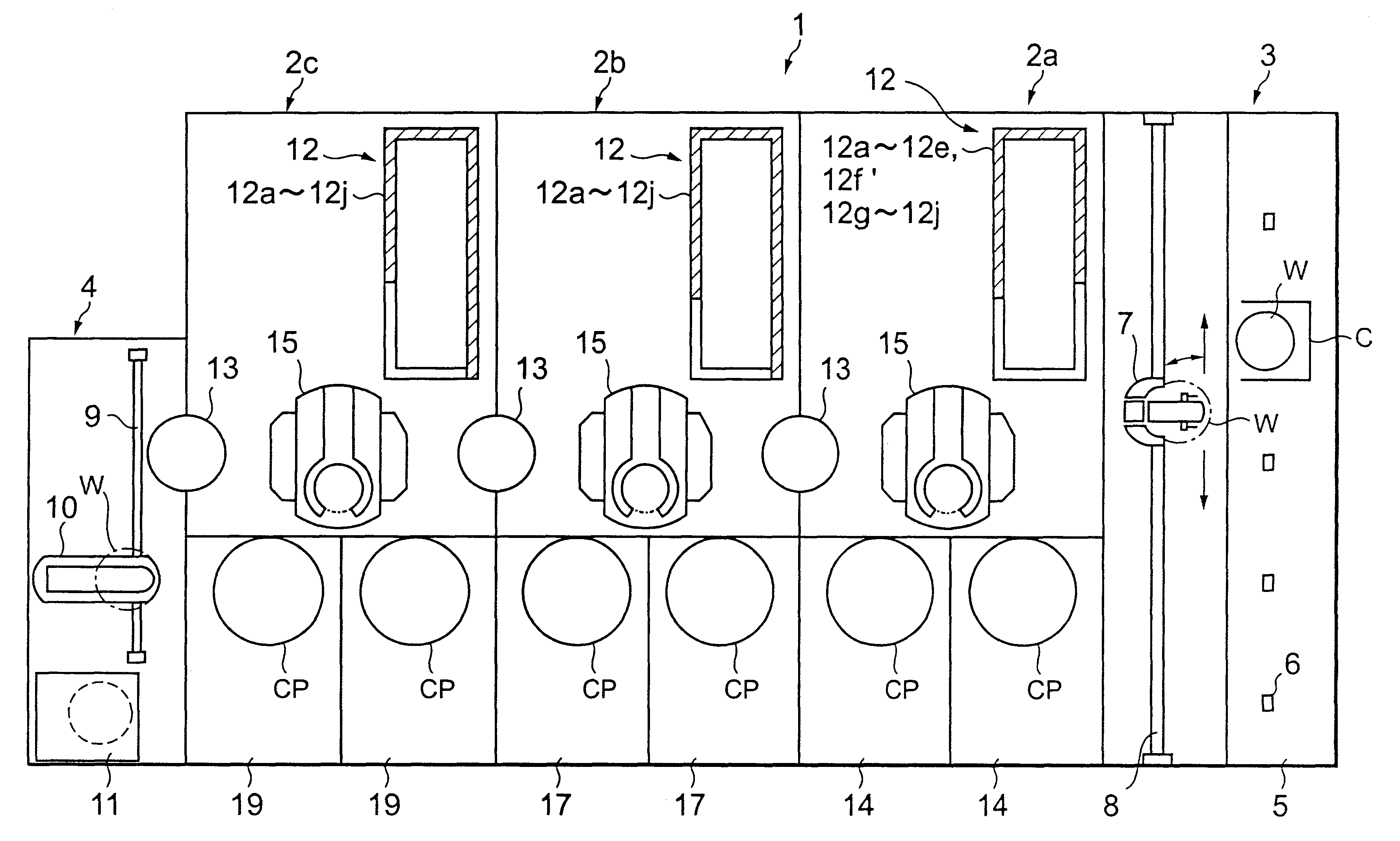
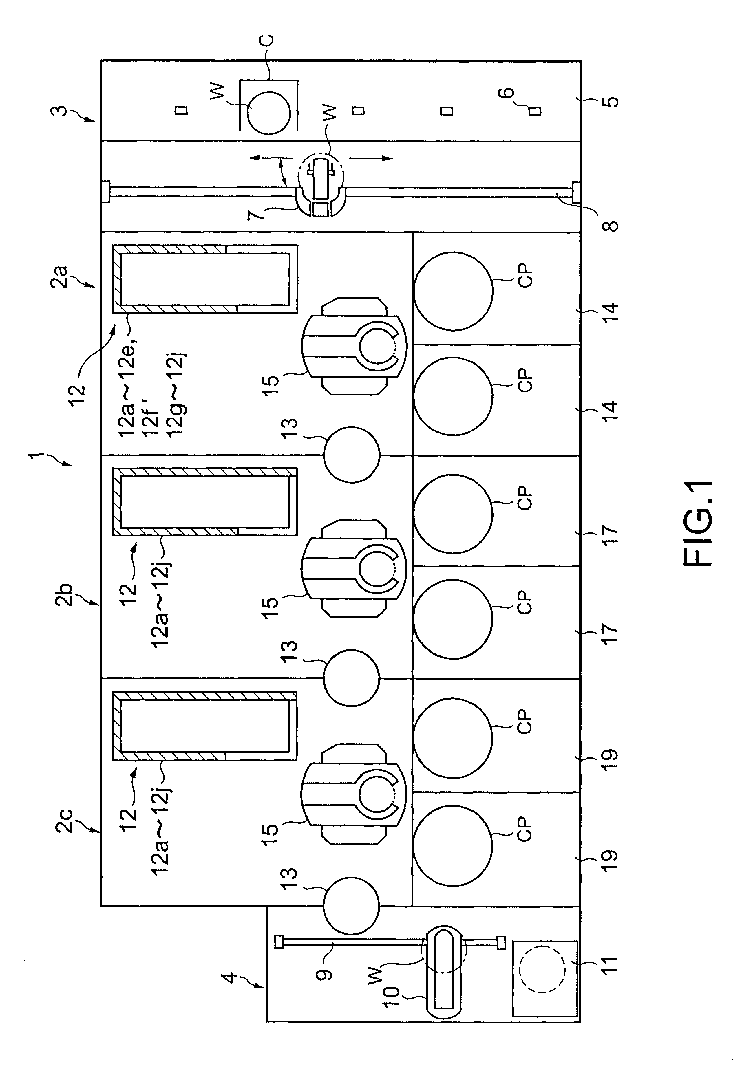
FIG. 1 is a plan view showing the structure of a coating and developing process system according to the present invention. FIG. 2 is a front view showing the structure of the coating and developing process system shown in FIG. 1. FIG. 3 is a rear view showing the structure of the coating and developing process system shown in FIG. 1.
In FIGS. 1, 2, and 3, a coating and developing process system 1 has a plurality of (for example three) process stations 2a, 2b, and 2c that are connected in parallel in such a manner that the second process station 2b is disposed between the first and third process stations 2a and 2c. A cassette station 3 is disposed outside the first process station 2a. The cassette station 3 loads and unloads a cassette C that accommodates for example 25 wafers W to / from the coating and developing process system 1. In addition, the cassette station 3 loads and unloads a wafer W to / from a cassette C. An interface portion 4 is disposed outside the third process station 2...
second embodiment
Next, the present invention will be described.
FIG. 12 is a plan view showing the structure of a coating and developing process system according to the second embodiment of the present invention. For simplicity, in FIG. 12, similar portions to those in the first embodiment are denoted by similar reference numerals.
As shown in FIG. 12, a coating and developing process system 51 has process stations 51a, 51b, and 51c that are connected in parallel as a second process unit. The structure of each of the process stations 51a, 51b, and 51c is different from the structure of the process stations 2a, 2b, and 2c of the first embodiment. In addition, the structure of each of process units 53, 54, and 55 of the second embodiment is different from the structure of each of the process units 53, 54, and 55 of the first embodiment.
FIG. 13 is a side view showing an outlined structure of each of the process units 53, 54, and 55.
As shown in FIG. 13, a cooling process plate 61 is disposed on one side (...
third embodiment
Next, the present invention will be described.
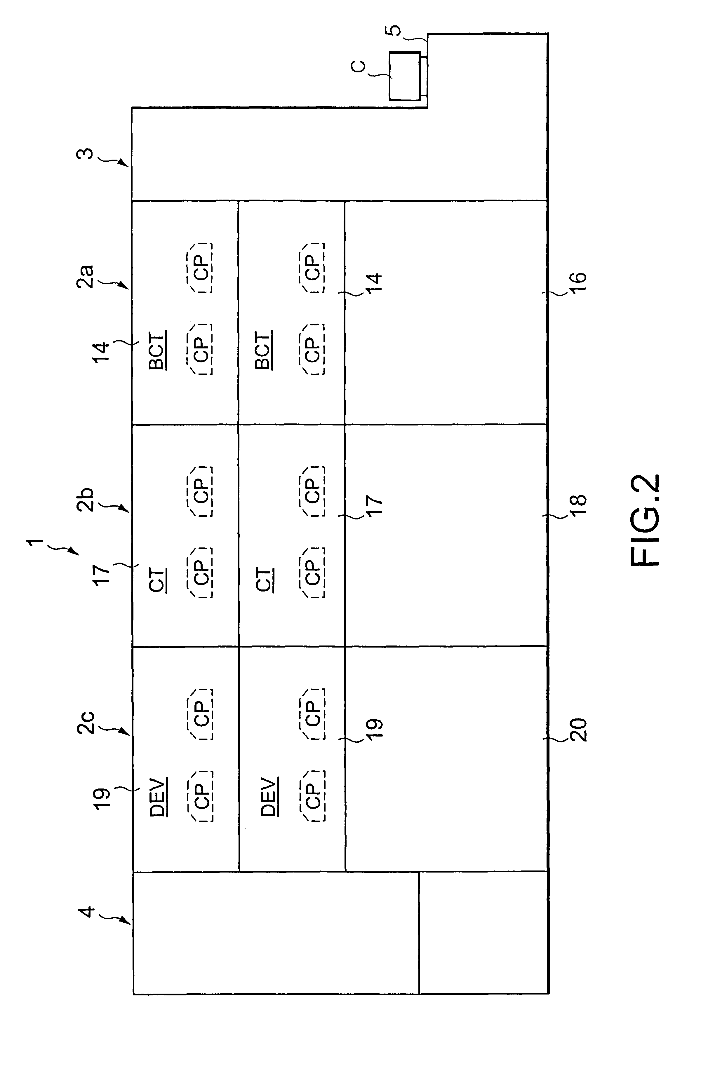
FIG. 14 is a plan view showing the structure of a coating and developing process system according to the third embodiment of the present invention. FIG. 15 is a front view of the coating and developing process system. In FIG. 14 and 15, similar portions to those in the first embodiment are denoted by similar reference numerals.
As shown in FIGS. 14 and 15, the structure of each of process stations 72a, 72b, and 72c of a coating and developing process system 71 is different from the structure of each of the process stations 2a, 2b, and 2c of the first embodiment. In the process station 72a, four-staged process units (BCT) 14 are disposed at a front portion of the process station 72a. In the process station 72b, four-staged process units (CT) 17 are disposed at a front portion of the process station 72b. In the process station 72c, four-staged process units (DEV) 19 are disposed at a front portion of the process station 72c. A solution supp...
PUM
 Abstract
Description
Claims
Application Information