Electron multiplier

a technology of electron multiplier and electron microscope, which is applied in the field of electron multiplier and electron multiplier, can solve the problems of increasing size and cost, complicated apparatus,

Inactive Publication Date: 2001-07-24
HAMAMATSU PHOTONICS KK
View PDF12 Cites 43 Cited by
  • Summary
  • Abstract
  • Description
  • Claims
  • Application Information

AI Technical Summary

Problems solved by technology

Consequently, the apparatus becomes complicated, thereby increasing the size and cost thereof.
In particular, the conventional structure for mounting the electron multiplier h

Method used


Image

  • Electron multiplier
  • Electron multiplier
  • Electron multiplier

Examples


first embodiment

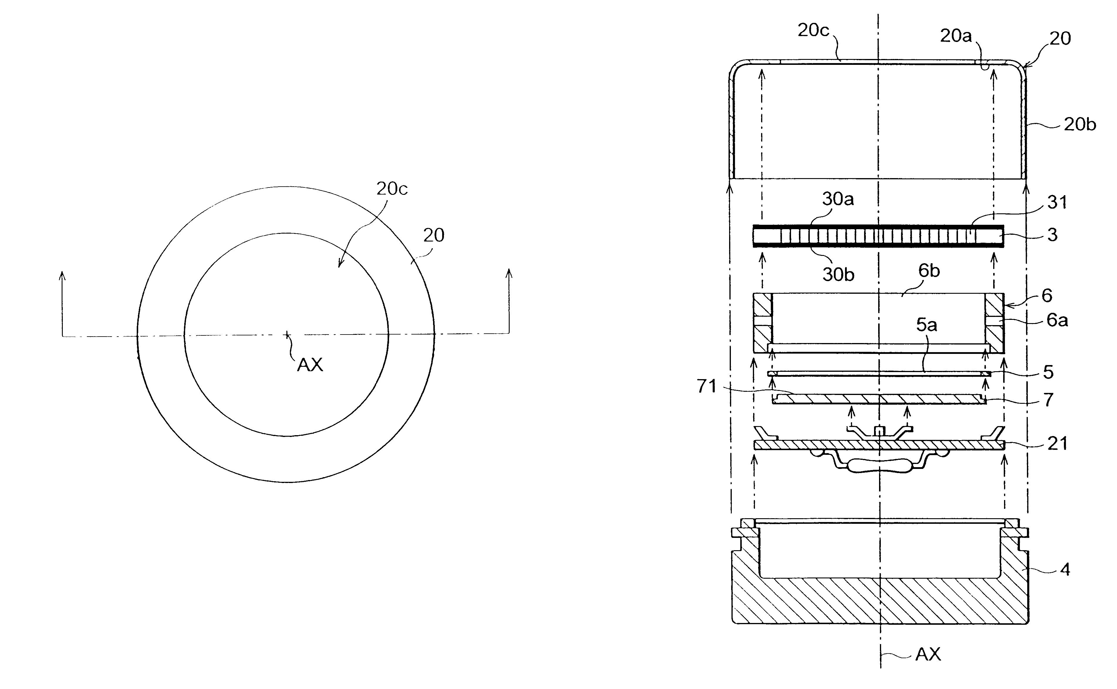
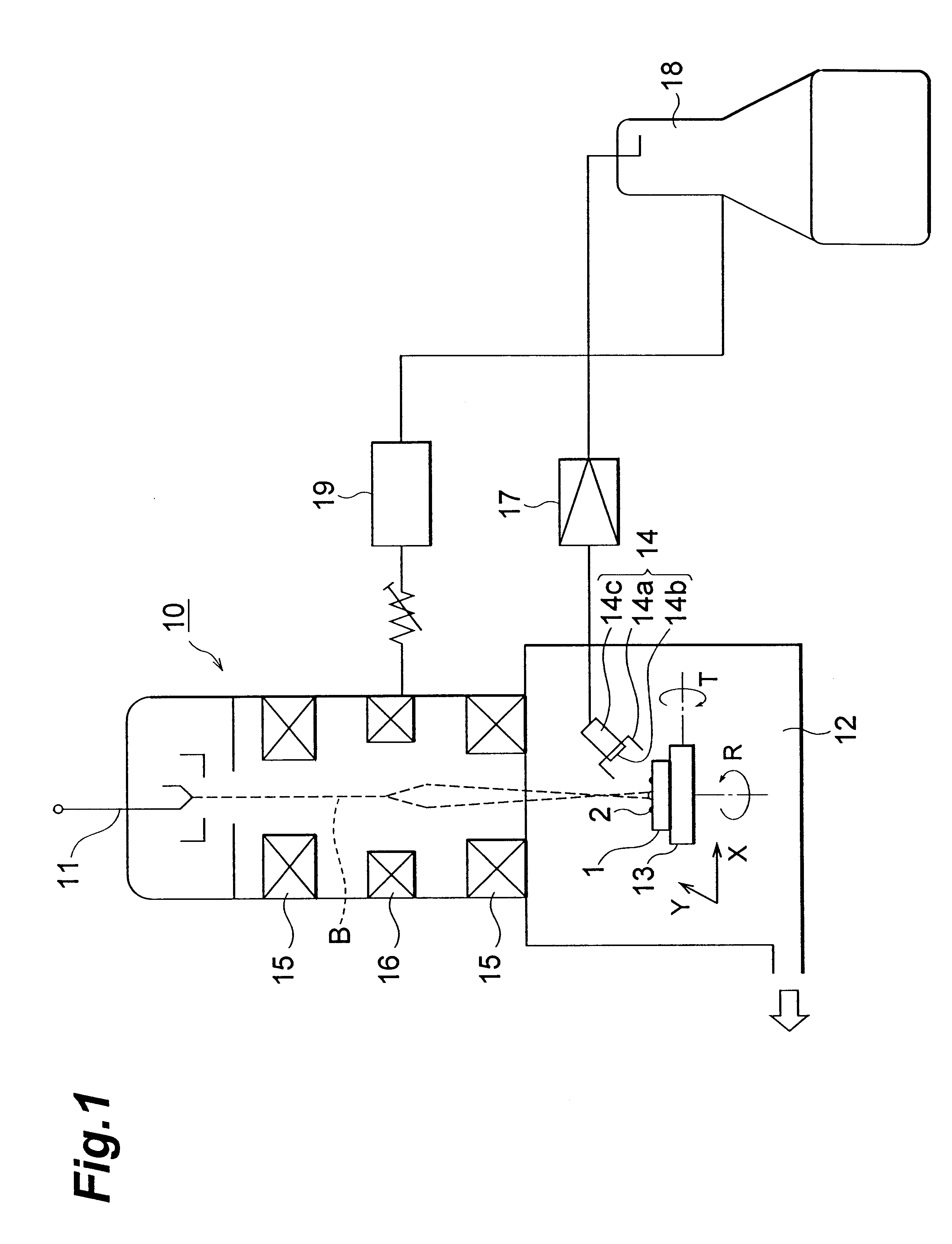
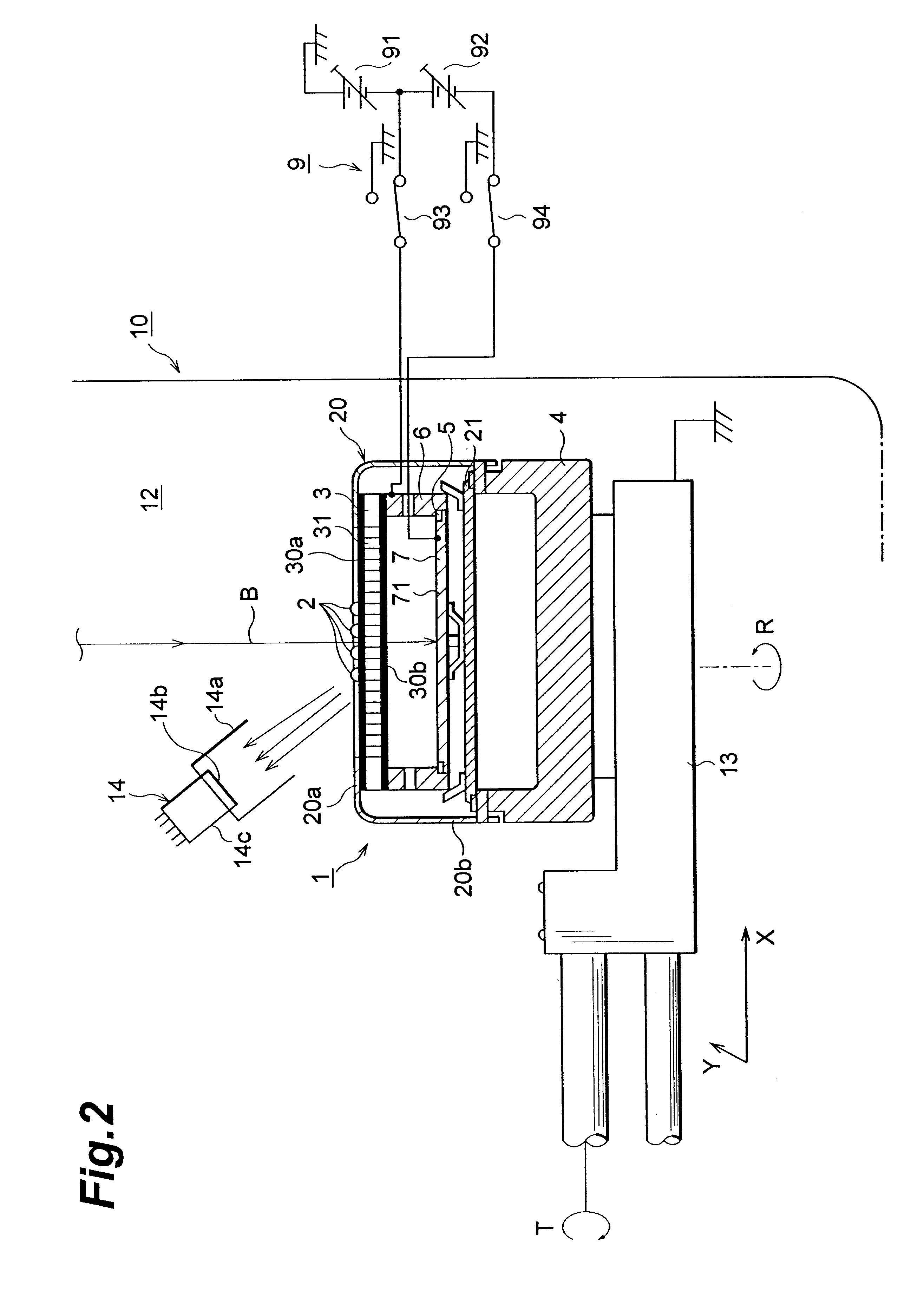
A first embodiment of the electron multiplier 1 according to the present invention will now be explained with reference to FIGS. 2 to 7. FIG. 2 is a sectional view showing the schematic configuration (including a voltage supply system) of the electron multiplier according to the present invention in the state where it is employed in the electron microscope shown in FIG. 1. FIG. 3 is a plan and assembling view showing a major part of the electron multiplier 1 shown in FIG. 2, wherein each member is illustrated by a sectional view taken along the line I--I of the plan view. FIG. 4 is a view, identical to the plan and assembling view shown in FIG. 3, showing the major part of the electron multiplier according to the present invention, whose lines are partly omitted in order to clarify the cross-sectional form of each member. FIG. 5 is a sectional view showing the schematic configuration of the first embodiment of the electron multiplier according to the present invention. FIG. 6 is a v...


PUM


Abstract

The present invention relates to an electron multiplier including a structure which effectively prevents an electric field from leaking to the front side of an MCP due to a voltage applied to the MCP, facilitates an operation of attaching/detaching the MCP, and prevents the MCP from being damaged and so forth during the operation. The electron multiplier includes an MCP as electron multiplying means, and an outer electric field shield member for accommodating the MCP. The electric field shield cap includes a body portion surrounding at least a side face of the MCP. The electron multiplier further includes a structure by which, while the MCP is held by the outer electric field shield member and an inner electric field shield member accommodated in the outer electric field shield member, the outer electric field shield member is attached to a base of the electron multiplier so as to facilitate the operation of attaching/detaching the MCP.

Description

DESCRIPTION1. Technical FieldThe present invention relates to a device applicable, for example, to electron microscopes; and, in particular, to an electron multiplier for multiplying incident electrons and outputting thus multiplied electrons.2. Background ArtAs conventional electron microscopes, those of reflection type and transmission type have been known. To these electron microscopes, an electron multiplier equipped with a microchannel plate (hereinafter referred to as MCP) having a plurality of channels for electron multiplication is applicable as electron multiplying means.Here, the reflection type electron microscope is an apparatus which detects secondary electrons from a sample generated by an electron beam emitted toward the sample, and processes the resulting signal, so that an image of the sample is observed. On the other hand, the transmission type electron microscope is an apparatus which detects electrons transmitted through a sample irradiated with an electron beam,...

Claims


Application Information

Patent Timeline
IPC IPC(8): H01J37/244H01J43/24H01J43/00
CPCH01J43/246H01J37/244
Inventor WATANABE, HIROYUKIKUSUYAMA, YUTAKAIGUCHI, MASAHIKO
Owner HAMAMATSU PHOTONICS KK
Why Eureka
Try Eureka