Method of fabricating MOSFET with lateral resistor with ballasting

a technology of lateral resistor and ballasting, which is applied in the direction of resistors, semiconductor devices, electrical equipment, etc., can solve the problems of increasing resistive losses with attendant temperature increase, poor conductors of heat, and increasing curren

Inactive Publication Date: 2001-07-31
IBM CORP +1
View PDF14 Cites 21 Cited by
  • Summary
  • Abstract
  • Description
  • Claims
  • Application Information

AI Technical Summary

Benefits of technology

It is another object of the invention to provide a transistor structure which will allow maximum integration density with minimal, if any, compromise of potential benefits thereof in regard to performance, functionality and / or manufacturing economy.
It is a further object of the invention to provide a technique allowing the selective development of resistances and / or connections at near minimum lithographic feature sizes.
It is yet another object of the invention to provide a transistor which has two salicide resistance phase states in a common structure for optimization of manufacturability, yield, performance and electrostatic discharge robustness.
It is yet another object of the invention to provide a transistor with lateral resistor ballasting, low series resistance and a low resistance gate salicide film by maintaining a high resistance salicide film in the vicinity of the transistor gate.

Problems solved by technology

Active devices must also be isolated from each other by insulator structures which generally surround the active devices and are poor conductors of heat.
Accordingly, increase of temperature due to resistive losses in a channel of an FET causes increase of current in the channel or a portion thereof and further increases resistive losses with attendant temperature increase.
If heat is not conducted away from the conduction region in sufficient degree to stabilize the semiconductor temperature, a phenomenon known as thermal runaway may occur, rendering the transistor inoperative for switching functions and often destroying the transistor structure.
For example, a transistor used to precharge a dynamic circuit prior to an input signal evaluation may be very narrow since the current drive requirements are very low.
The existence of a thermal gradient from the center to the edges of the channel, when developed, implies stronger conduction at the center of the channel with attendant additional resistive losses near the center of the channel.
Therefore, the temperature and current near the center of the channel may become much larger than at the edges and, unless sufficient heat can be conducted through the channel to its edges and then away from the transistor to stabilize the thermal gradient and maximum temperature, thermal runaway and destruction of the transistor may result.
Accordingly, thermal dissipation properties of the transistor may be the principal limitation on transistor performance and operating conditions.
Unfortunately, at high integration density and small device sizes, particularly when integrated circuit designs include isolation structures, the individual active devices have very small thermal mass while heat removal from the FET channel regions may be limited.
Further, it should be recognized that integration density is generally limited by lithographic resolution at any given minimum feature size regime.
Therefore, any structure of minimum feature size or larger directed to controlling thermal conditions or "ballasting" to balance voltage and current conditions within an individual transistor implies a relatively large transistor size and compromise or limitation of integration density that could otherwise be achieved.
That is, in summary, circuit performance. functionality and manufacturing economy goals may impose limitations on performance of individual transistors which, in turn, impose limitations of the circuit performance goal which may be achieved while worst case transistor operating conditions may limit the realization of integrated circuit performance and reliability criteria which could otherwise be achieved at any given minimum lithographic feature size regime.
The contact size limitation, however, has not been significant at lower integration densities than are currently being developed.
Further, no exploitation of this effect to achieve meritorious or beneficial electrical characteristics or any other semiconductor device design advantage or attribute has been proposed.

Method used


Image

  • Method of fabricating MOSFET with lateral resistor with ballasting
  • Method of fabricating MOSFET with lateral resistor with ballasting
  • Method of fabricating MOSFET with lateral resistor with ballasting

Examples


Embodiment Construction

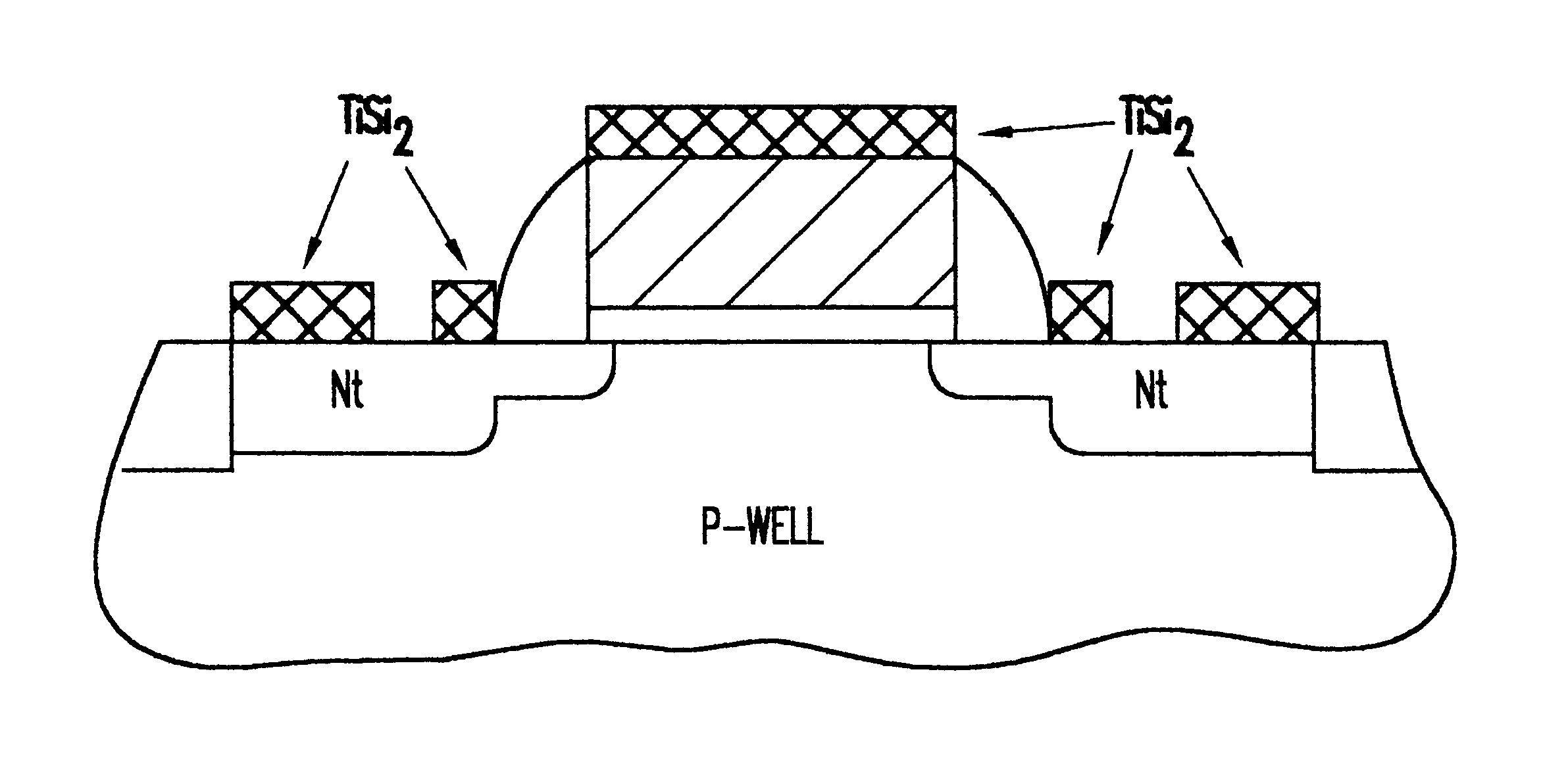
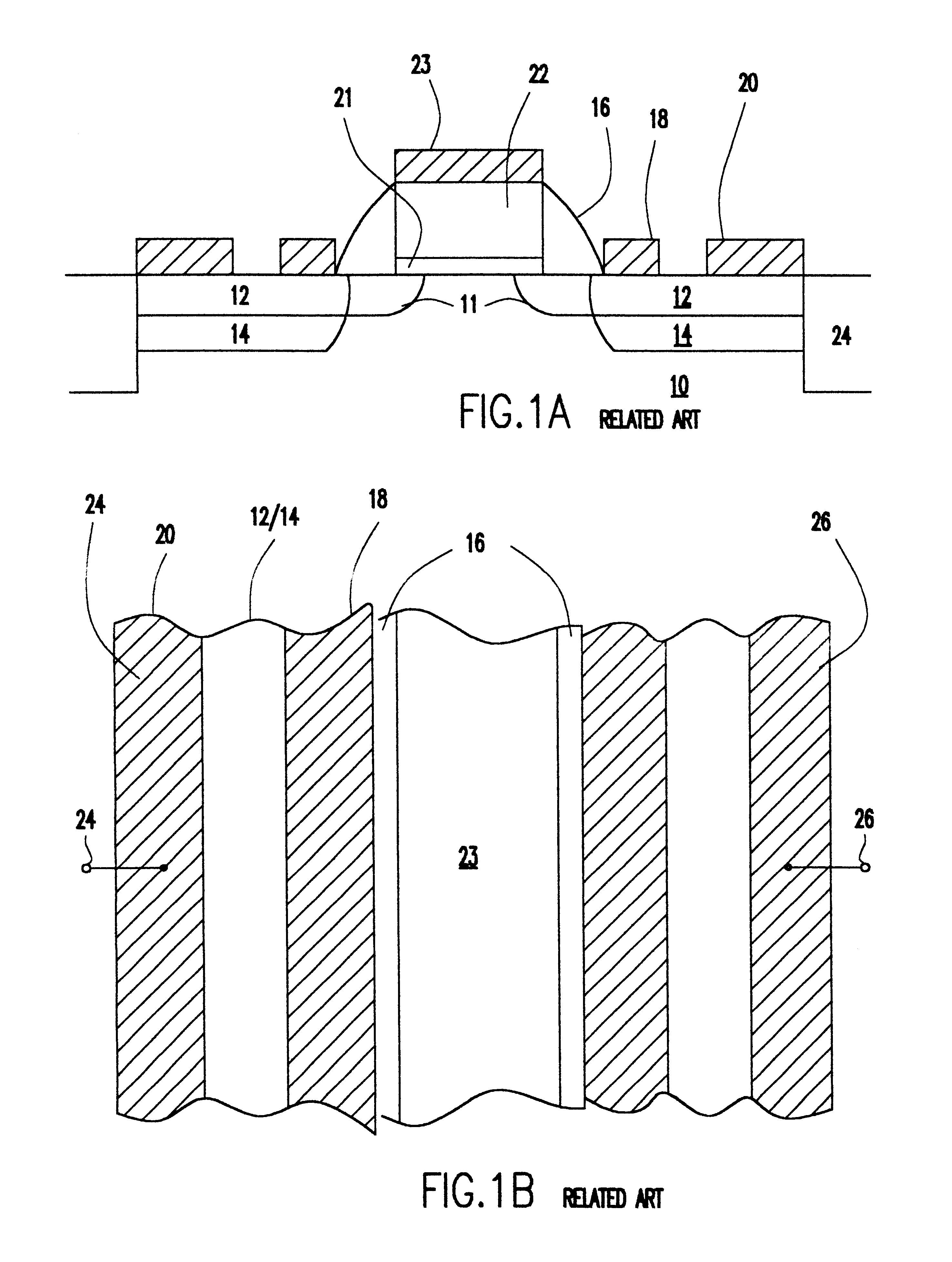
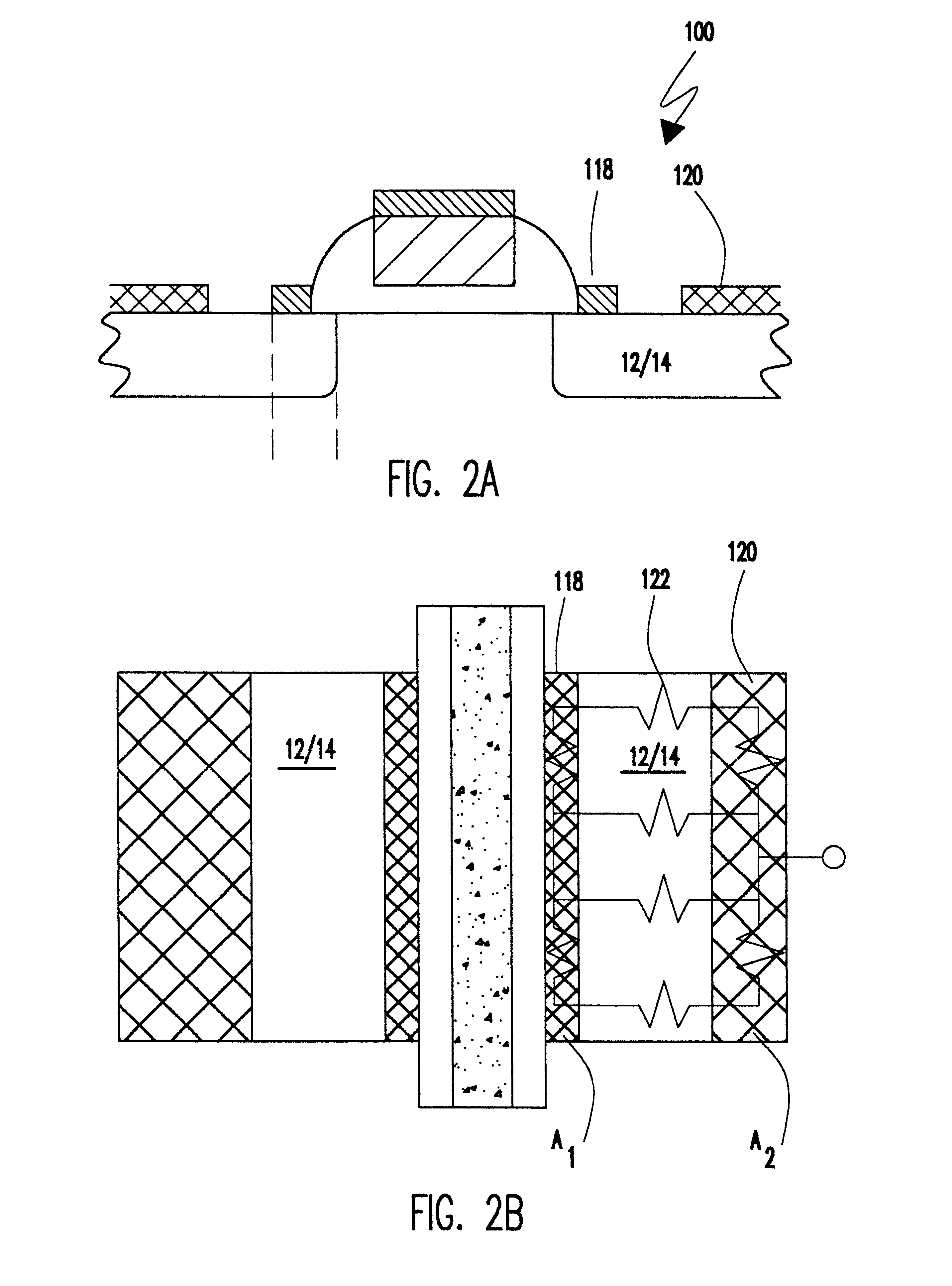
Referring now to the drawings, and more particularly to FIGS. 1A and 1B, there is shown in cross-section and plan view, respectively, a structure of a current FET design over which the present invention provides an improvement. It is to be understood that the invention may be considered to utilize some features of the design of FIGS. 1A and 1B but at a different size relative to minimum feature size as well as different materials having different electrical properties controllable in accordance with the present invention. Further, FIGS. 1A and 1B are arranged to facilitate conveyance of an understanding of the invention rather than to depict details of any particular known design. Therefore, FIGS. 1A and 1B are designated as being "Related Art" and no portion of either Figure is admitted to be Prior Art in regard to the present invention.

As shown in FIGS. 1A and 1B, a field effect transistor is formed partially within a substrate 10 by implantation of source and drain regions 12 in ...


PUM


Abstract

The current density profile in the conduction channel of a field effect transistor is controlled and thermal gradients are limited under extreme operating conditions by providing lateral resistive ballasting at the source / drain regions adjacent the conduction channel. A distributed resistance is formed by inhibiting conversion of a region of deposited salicide from a high resistance phase state to a low resistance phase state through formation of the deposit with a width or area less than a critical dimension.

Description

1. Field of the InventionThe present invention generally relates to high density integrated circuits and, more particularly, to regulating performance and conduction characteristics of MOSFET devices included therein.2. Description of the Prior ArtThe enhancements to performance and economy of manufacture derived from high density integration of semiconductor integrated circuits have been recognized for several years. During this same period of time, field effect transistor (FET) technology has generally become the technology of choice for all but the most critical of applications in view of scalability of field effect transistors to small sizes consistent with conduction requirements and other properties facilitating process economy, integration density and high manufacturing yield as well as exhibiting good operating margins and low drive current requirements. Field effect transistors function as switching device by using a field developed by a voltage on an insulated gate to cont...

Claims


Application Information

Patent Timeline
Patent Type & Authority Patents(United States)
IPC IPC(8): H01L21/02H01L21/336H01L21/285H01L29/43H01L29/40H01L29/417H01L27/07
CPCH01L21/28518H01L27/0738H01L29/665H01L29/41725H01L29/435H01L28/24
Inventor GAUTHIER, JR., ROBERT J.MANN, RANDY W.VOLDMAN, STEVEN H.
Owner IBM CORP
Why Eureka
Try Eureka