Chemical mechanical polish (CMP) planarizing method with enhanced chemical mechanical polish (CMP) planarized layer planarity

Inactive Publication Date: 2001-08-07
TAIWAN SEMICON MFG CO LTD
View PDF8 Cites 5 Cited by
  • Summary
  • Abstract
  • Description
  • Claims
  • Application Information

AI Technical Summary

Problems solved by technology

While chemical mechanical polish (CMP) planarizing methods are in particular desirable within the art of microelectronic fabrication for fabricating microelectronic layers with enhanced planarity, chemical mechanical polish (CMP) planarizing methods are also not entirely without problems within the art of microelectronic fabrication insofar as chemical mechanical polish (CMP) planarizing methods do not always provide an optimally planar surface of a chemical mechanical polish planarized layer within a microelectronic fabrication.

Method used


Image

  • Chemical mechanical polish (CMP) planarizing method with enhanced chemical mechanical polish (CMP) planarized layer planarity
  • Chemical mechanical polish (CMP) planarizing method with enhanced chemical mechanical polish (CMP) planarized layer planarity

Examples


Embodiment Construction

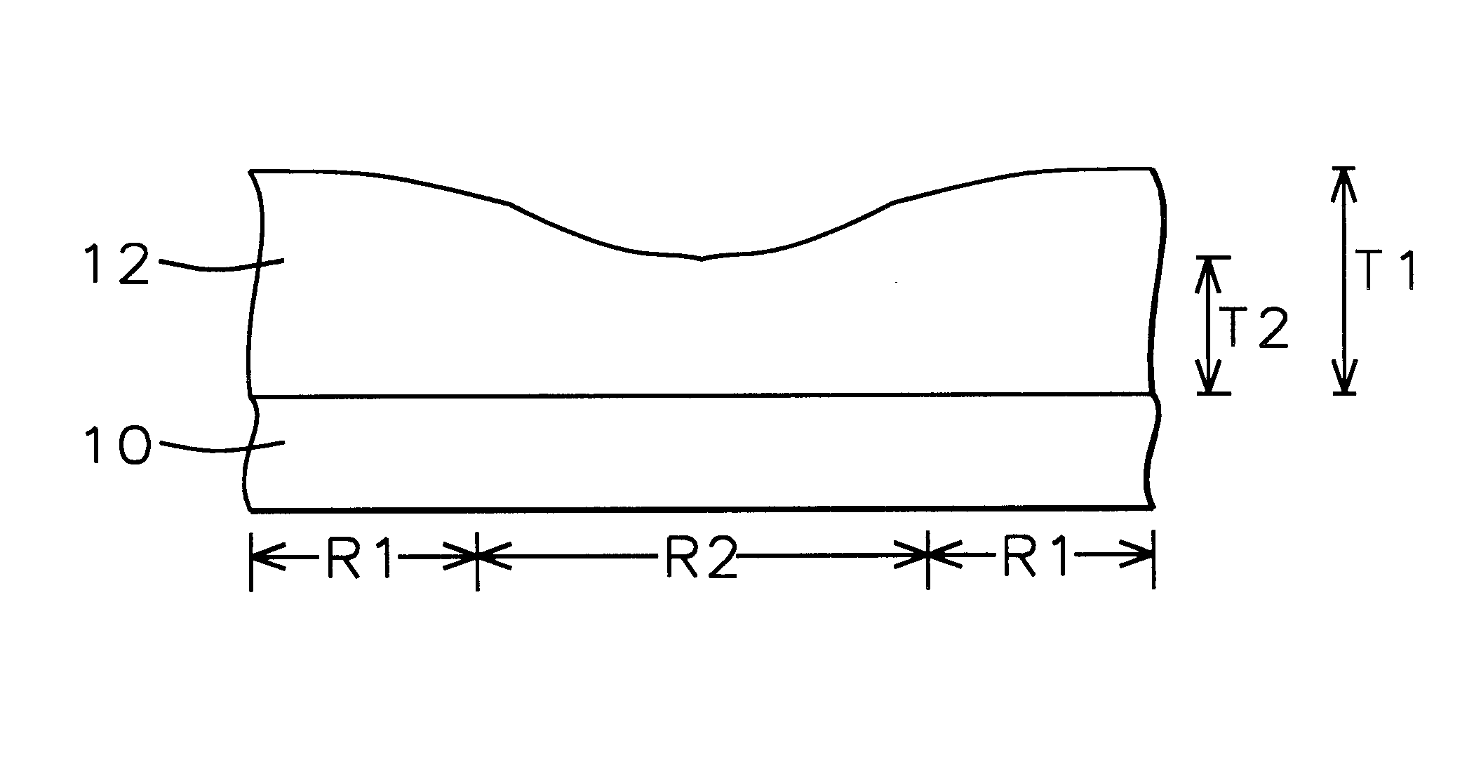
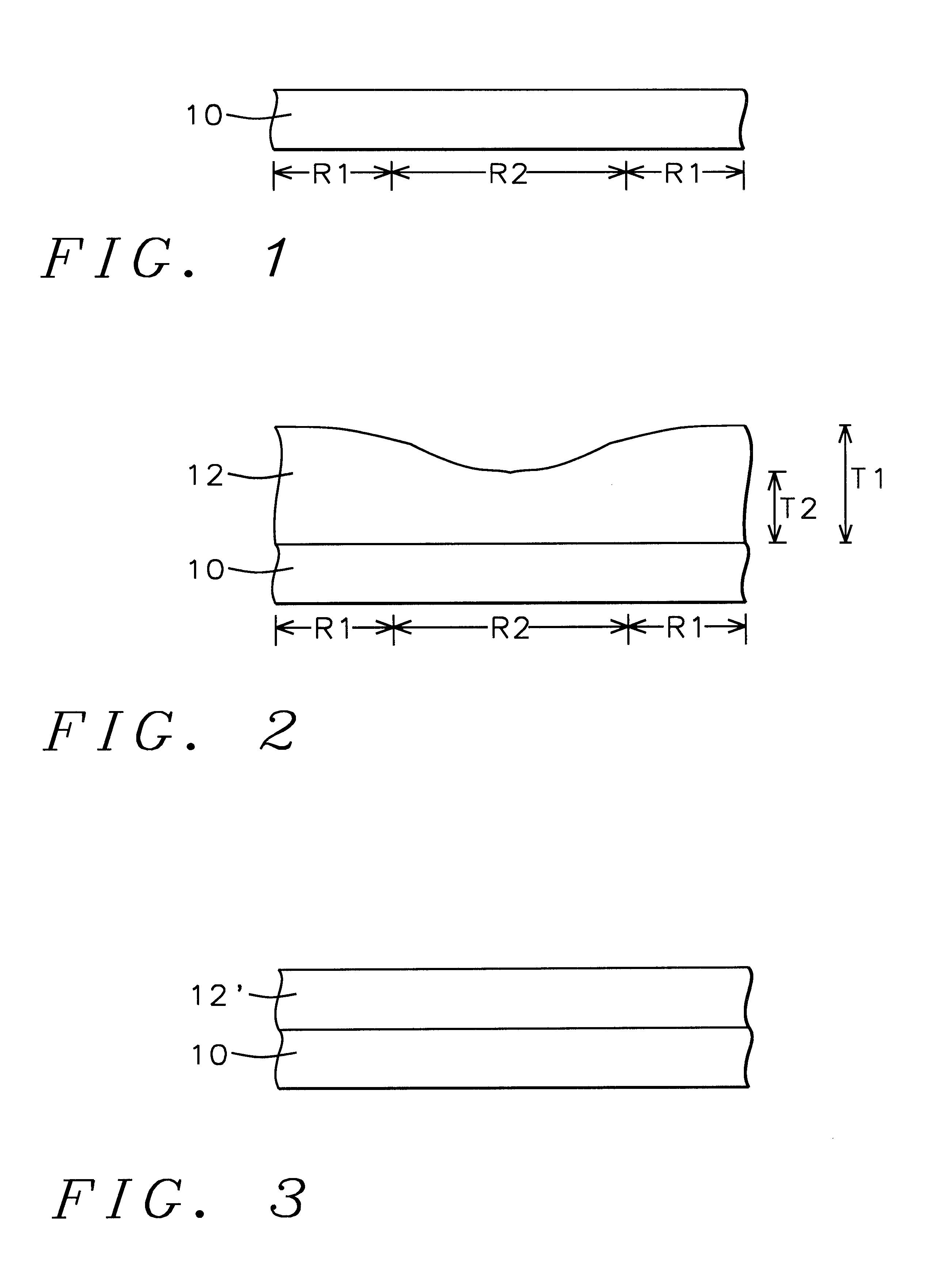
There was obtained an eight inch diameter (100) silicon semiconductor substrate which was fixtured into an apparatus which employed a high density plasma chemical vapor deposition (HDP-CVD) method for forming a dielectric layer upon the eight inch diameter (100) silicon semiconductor substrate. A high density plasma chemical vapor deposition (HDP-CVD) method is understood by a person skilled in the art to be a plasma enhanced chemical vapor deposition (PECVD) method undertaken simultaneously with an inert gas sputtering method, where a deposition rate within the plasma enhanced chemical vapor deposition (PECVD) method exceeds a sputtering rate within the inert gas sputtering method. The eight inch diameter (100) silicon semiconductor substrate was fixtured upon a thermally conductive chuck which provided: (1) a temperature of about 420 degrees centigrade at an annular edge region of the silicon semiconductor substrate of annular width of about 30 millimeters which included the circu...


PUM

PropertyMeasurementUnit
Temperatureaaaaaaaaaa
Thicknessaaaaaaaaaa
Dielectric polarization enthalpyaaaaaaaaaa

Abstract

A chemical mechanical polish (CMP) planarizing method for forming a chemical mechanical polish (CMP) planarized microelectronic layer within a microelectronic fabrication employs first a substrate. There is then formed over the substrate a microelectronic layer. There is then planarized, while employing a chemical mechanical polish (CMP) planarizing method, the microelectronic layer to form a chemical mechanical polish (CMP) planarized microelectronic layer. Within the method, the microelectronic layer when formed over the substrate is formed with a thickness variation which compensates for a chemical mechanical polish (CM) rate non-uniformity when forming while employing the chemical mechanical polish (CMP) planarizing method the chemical mechanical polish (CMP) planarized microelectronic layer from the microelectronic layer.

Description

1. Field of the InventionThe present invention relates generally to methods for forming planarized layers within microelectronics fabrications. More particularly, the present invention relates to chemical mechanical polish (CMP) planarizing methods for forming planarized layers within microelectronics fabrications.2. Description of the Related ArtMicroelectronic fabrications are formed from microelectronic substrates over which are formed patterned microelectronic conductor layers which are separated by microelectronic dielectric layers.As microelectronic fabrication integration levels have increased and microelectronic device and patterned microelectronic conductor layer dimensions have decreased, it has become more common within the art of microelectronic fabrication to employ within microelectronic fabrications multiple vertically disposed patterned microelectronic conductor layers within a microelectronic fabrication in order to provide for greater functionality within the micro...

Claims


Application Information

Patent Timeline
IPC IPC(8): H01L21/02H01L21/3105
CPCH01L21/31053
Inventor CHANG, WENGJANG, SYUN-MING
Owner TAIWAN SEMICON MFG CO LTD
Why Eureka
Try Eureka