This helps you quickly interpret patents by identifying the three key elements:
Problems solved by technology
Method used
Benefits of technology
Benefits of technology
The invention simplifies the process of aligning chip pads with substrate pads by providing alignment markings which can be simultaneously or sequentially viewed from a single direction. Further, the alignment markings are chip-based and are not external to the chip. Thus, the invention dramatically simplifies the alignment process and reduces the need for prism-based alignment mechanisms, transparent substrates or other complicated and expensive conventional alignment technologies. Further, the invention reduces or eliminates the need for electrical alignment testing of the pad connections by providing alignment marks which remain visible from a single viewing location after the chip is attached to the substrate.
Problems solved by technology
It is difficult to place chips, such as flip chips and other surface mounted devices and packages, accurately since the signal and attachment pads are between the carrier package (or circuit board) and the chip / package during placement.
Such conventional techniques and devices are expensive and difficult to use from both hardware and control logic standpoints.
Further, the placement and confident verification requires high degrees of mechanical, optical, and control system sophistication.
Method used
Image
Click on the blue label to locate the original text in one second.
Reading with bidirectional positioning of images and text.
Examples
first embodiment
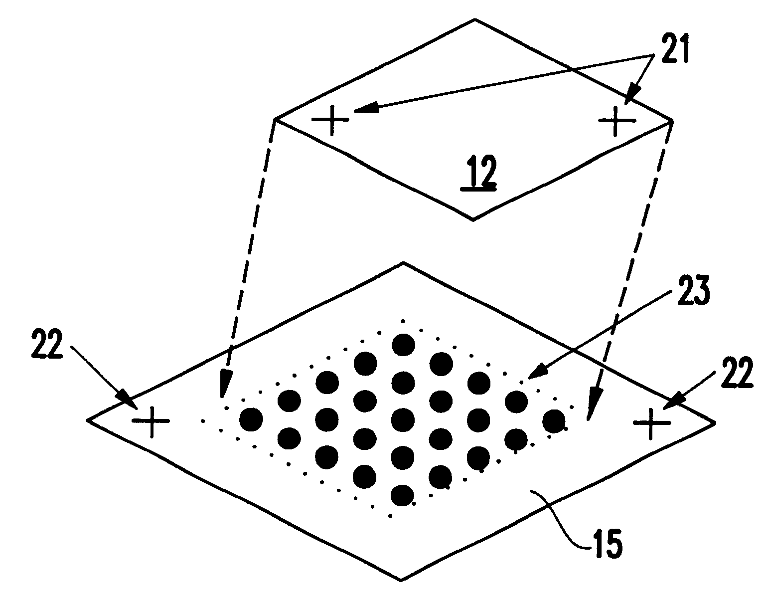
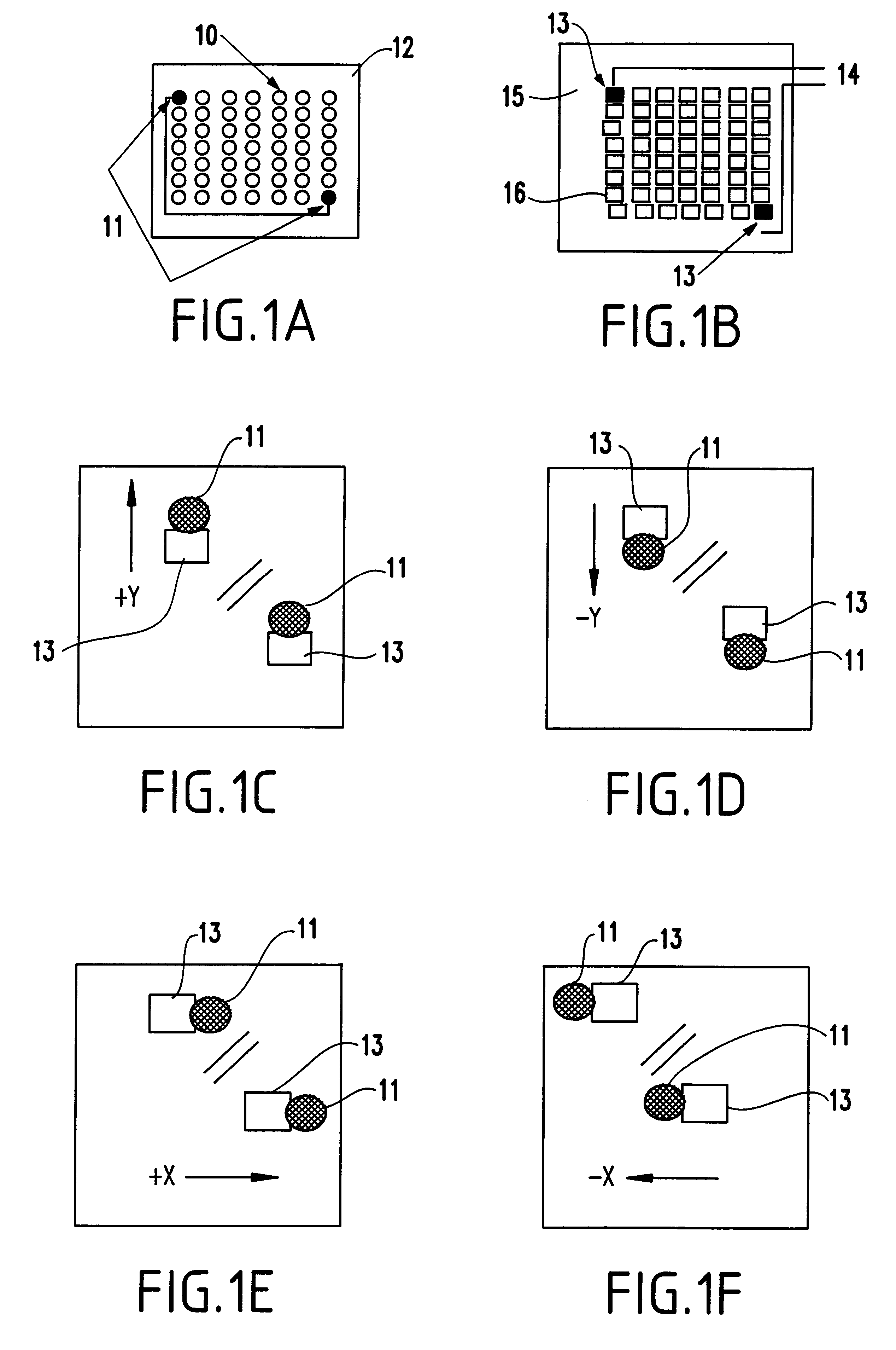
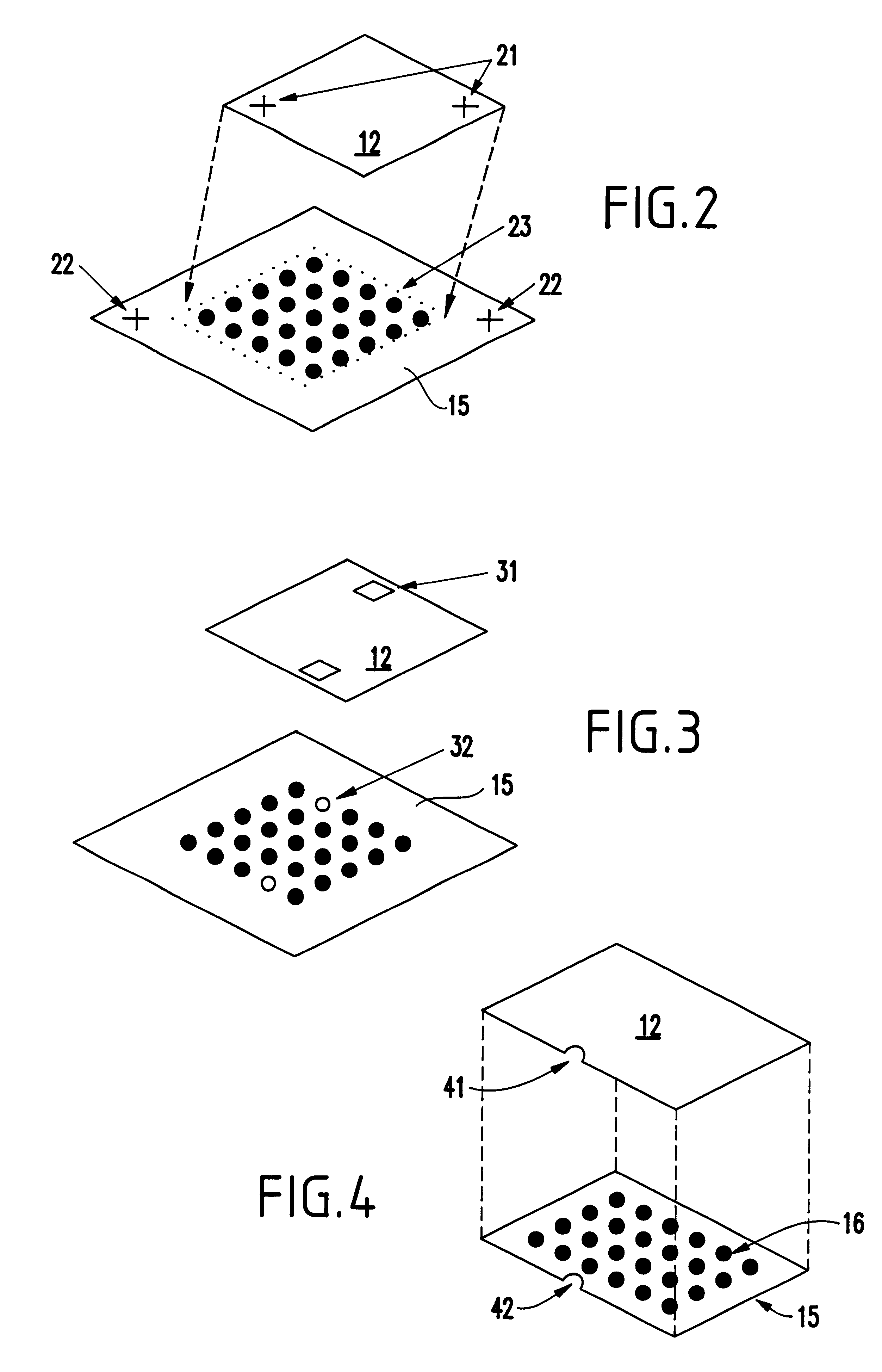
Referring now to the drawings, and more particularly to FIGS. 1A-1F, the invention is illustrated. FIG. 1A illustrates a connection side (e.g., lower or front side) of a chip 12 (e.g., semiconductor or other integrated circuit chip, such as a flip-chip or other similar devices) and FIG. 1B illustrates the connection side (e.g., upper or back side) of a substrate 15 (such as a rigid or flexible semiconductor substrate).
The chip pads 10 (e.g., conductors) are aligned and electrically connected to the substrate pads 16 by solder reflow, thermo-compression, or conductive adhesives, as discussed above. As also discussed above, the pads 10, 16 are input / output devices which allow signals to be transferred between the substrate 15 and the chip 12.
To verify alignment of the chip 12 and substrate 15, chip alignment pads connect with substrate alignment pads 13. As shown in FIGS. 1C-1F, the alignment pads 11, 13 will be aligned in the + / -Y-directions (FIGS. 1C-1D) and in the + / -X-directions (...
second embodiment
the invention produces advantages similar to the first embodiment by allowing visual inspection of the alignment of the chip pads and the substrate pads 15 from a single viewing location. As with the previous embodiment, the invention reduces the complexity of the alignment and attachment process and increases the ease of post-attachment inspection. Once again, these advantages are obtained because the alignment feature is chip-based and not external to the chip.
third embodiment
the invention is illustrated in FIG. 4. Again, in FIG. 4, the chip 12 and the substrate 15 are shown. However, in FIG. 4 the chip includes a chip alignment notch 41, and the substrate 15 includes a substrate alignment notch 42.
Again, as with the previous embodiments, the chip alignment notch 41 corresponds to the location of the chip pads 10. The substrate alignment notch 42 similarly corresponds to the substrate pads 16. Therefore, when the alignment notches 41, 42 are aligned, the chip pads 10 and the substrate pads 16 will also be aligned.
The notches 41, 42 accurately map the chip edge to the chip pad locations. A placement tool could use these notches 41, 42 as references to align the chip pads 10 with the substrate pads. The sides of the chip 12 and substrate 15 could be accurately diced or re-diced to provide the accurate edge relationship to the chip pads. Only enough of two edges need to be used for the placement. Thus, partially dressed edges would be consistent with the in...
PUM
Abstract
A method and structure for manufacturing semiconductor devices comprising providing a chip and a substrate, aligning the chip and the substrate, attaching the chip to the substrate and optionally verifying chip / substrate alignment, the aligning comprising providing at least one chip alignment mark on a first side of the chip (wherein the chip alignment mark corresponds to chip pads on a second side of the chip) and aligning the alignment mark with substrate pads on the substrate.
Description
1. Field of the InventionThe present invention generally relates to a method for manufacturing solid-state devices and more particularly to method of using alignment marks on one side of a chip to determine locations of pads on the other side of the chip and to align the chip pads with substrate pads.2. Description of the Related ArtChip attachment technologies such as solder reflow, thermo-compression, and conductive adhesives are becoming mainstream processes for chip or integrated circuit device attachment. The advantages of surface mounted chips and other devices are well known to those skilled in the art. The most demanding aspect of chip / substrate assembly is generally regarded to be chip placement relative to the supporting substrate or board.It is difficult to place chips, such as flip chips and other surface mounted devices and packages, accurately since the signal and attachment pads are between the carrier package (or circuit board) and the chip / package during placement. ...
Claims
Application Information
Patent Timeline
Application Date:The date an application was filed.
Publication Date:The date a patent or application was officially published.
First Publication Date:The earliest publication date of a patent with the same application number.
Issue Date:Publication date of the patent grant document.
PCT Entry Date:The Entry date of PCT National Phase.
Estimated Expiry Date:The statutory expiry date of a patent right according to the Patent Law, and it is the longest term of protection that the patent right can achieve without the termination of the patent right due to other reasons(Term extension factor has been taken into account ).
Invalid Date:Actual expiry date is based on effective date or publication date of legal transaction data of invalid patent.

