Power amplifier

a power amplifier and power supply technology, applied in the direction of amplifier combinations, single-ended push-pull amplifiers, gain control, etc., can solve the problems of large-scale cut-off circuits and regulators, high power consumption devices, and inability to dispose of cut-off circuits or regulators

Inactive Publication Date: 2001-08-21
MURATA MFG CO LTD
View PDF3 Cites 41 Cited by
  • Summary
  • Abstract
  • Description
  • Claims
  • Application Information

AI Technical Summary

Problems solved by technology

However, such cut-off circuits and regulators are typically large-scale, high power consumption devices.
It is therefore not possible to dispose a cut-off circuit or regulator between the battery and supply terminal of the HBT power amplifier 500, and the supply terminal is directly connected to an internal battery.
The last transistor 505 can fail as a result of load fluctuations during battery charging as described below, but failure can also result from an overvoltage being applied to the collector of the last transistor 505.
Providing a feedback circuit 600 as described above to the input/output terminals of such a high output po

Method used


Image

  • Power amplifier
  • Power amplifier
  • Power amplifier

Examples


embodiment 2

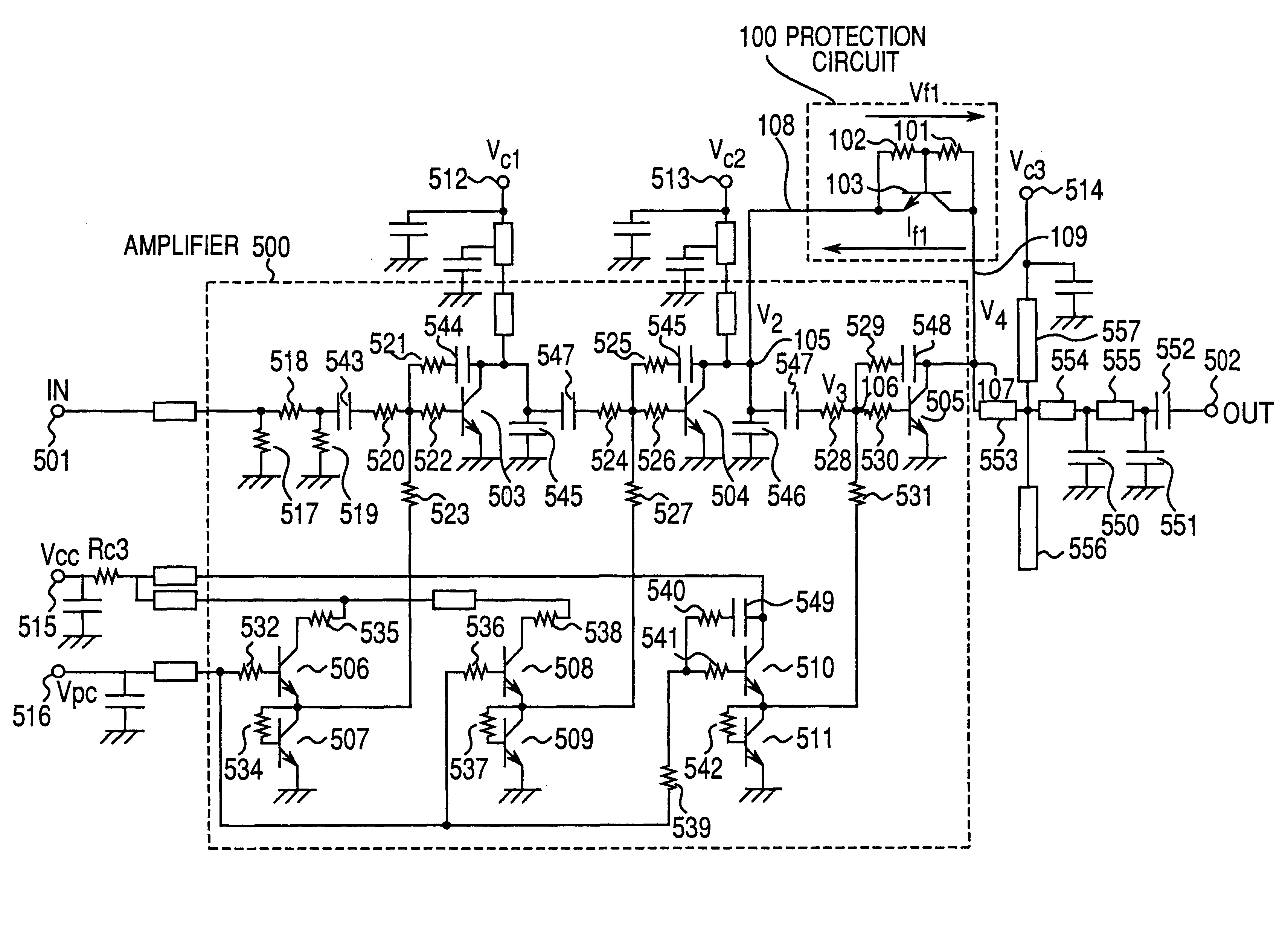
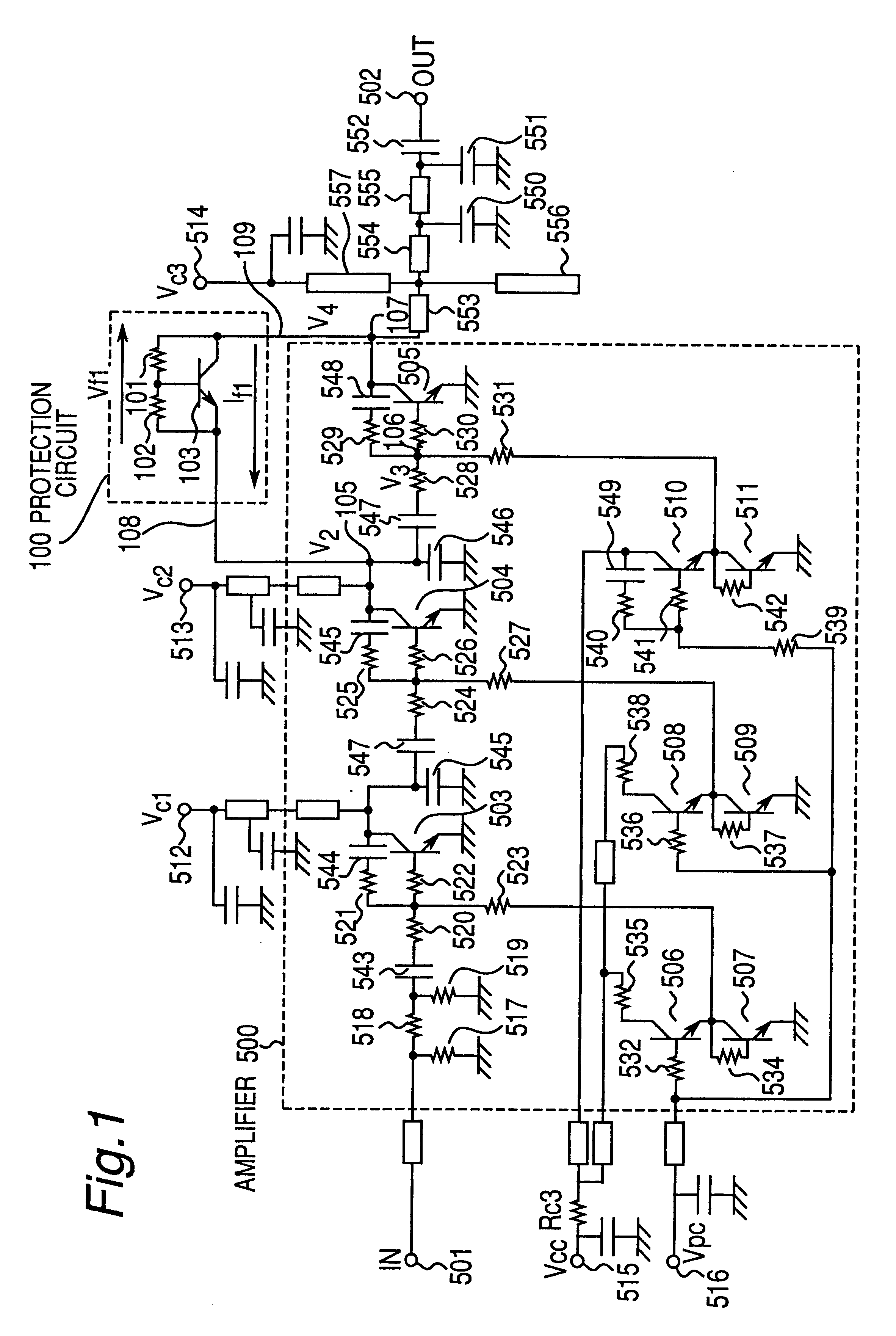
FIG. 4 is a circuit diagram of a protection circuit 130 according to a second preferred embodiment of the present invention used in the above-described power amplifier 500. Note that FIG. 4 shows only the significant circuit elements in the area of the second and third stage transistors 504 and 505 in power amplifier 500.

This protection circuit 130 comprises five transistors 131 to 135 diode connected in series with the collector of each transistor shorted to the base. The collector of transistor 131 is connected to terminal 137. This terminal 137 is connected to node 107 of power amplifier 500. The emitter of transistor 131-is connected to the collector of transistor 132. The emitter of transistor 132 is connected to the collector of transistor 133. The emitter of transistor 133 is connected to the collector of transistor 134. The emitter of transistor 134 is connected to the collector of transistor 135. The emitter of transistor 135 is connected to terminal 136, and terminal 136 i...

embodiment 3

FIG. 5 is a circuit diagram of a protection circuit 140 according to a third preferred embodiment of the present invention used in the above-described power amplifier 500. Note that FIG. 5 shows only the significant circuit elements in the area of the second and third stage transistors 504 and 505 in power amplifier 500.

As will be known from FIG. 5, this protection circuit 140 is substantially protection circuit 100 according to the first embodiment, further comprising a resistor 141 connected to the collector of transistor 103. Note that like parts in protection circuit 100 and this protection circuit 140 are identified by like reference numerals.

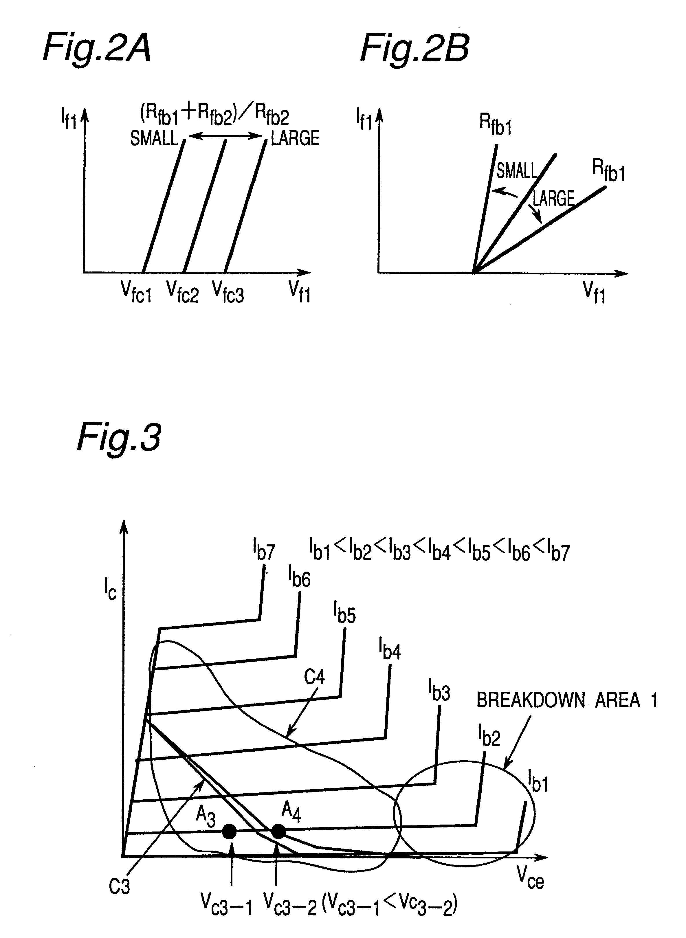
The on voltage of the protection circuit 140 thus comprised is (R.sub.fb1 +R.sub.fb2) / R.sub.fb2.times.1.3 (V). The on resistance can be adjusted by controlling resistance R.sub.fb1 of resistor 101 and R.sub.fc1 of resistor 141. It is therefore possible to more precisely control the feedback current. Other effects and achievements of this e...

embodiment 4

FIG. 6 is a circuit diagram of a protection circuit 150 according to a fourth preferred embodiment of the present invention used in the above-described power amplifier 500. Note that FIG. 6 shows only the significant circuit elements in the area of the second and third stage transistors 504 and 505 in power amplifier 500.

As will be known from FIG. 6, this protection circuit 150 is substantially protection circuit 100 according to the first embodiment, further comprising a resistor 151 connected to the emitter of transistor 103. Note that like parts in protection circuit 100 and this protection circuit 150 are identified by like reference numerals.

The on voltage of a protection circuit 150 thus comprised is (R.sub.fb1 +R.sub.fb2) / R.sub.fb2.times.1.3 (V). As with a protection circuit 140 according to the above third embodiment of the invention, the on resistance of this protection circuit 150 can be adjusted by controlling resistance R.sub.fb1 of resistor 101 and R.sub.fe1 of resistor...


PUM


Abstract

While minimizing any increase in chip size and without incurring a loss in performance or operating characteristic under normal operating voltage conditions, a power amplifier protection circuit effectively prevents breakdown of power amplifying transistors resulting from output load fluctuations during operation with an overvoltage supply. The protection circuit includes a gate circuit electrically connected between the collector and base of at least the last-stage transistor in a power amplifier including transistors connected in stages. The gate circuit passes a feedback current to the base electrode of the protected transistor when a voltage exceeding a specific level is applied to the collector of the protected transistor.

Description

1. Field of the InventionThe present invention relates to a protection circuit for preventing transistor breakdown during overvoltage output operation in a power amplifier having a GaAs heterojunction bipolar transistor (HBT) a Si bipolar transistor.2. Description of Related ArtMonolithic microwave integrated circuits (MMIC) and modules (hybrid ICs and multichip modules) using GaAs metal-semiconductor field effect transistors (MESFET), GaAs high electron mobility transistors (HEMT), or GaAs-based HBTs are widely used in power amplifiers for mobile communications devices. Of these, GaAs-based HBTs offer the following three advantages over conventional FETs, and are therefore considered promising as power module elements for future mobile communication devices. That is, a GaAs-based HBT:1) does not require a negative gate bias voltage, and can therefore be used for simple power supply operations;2) can be used for on / off operations without an analog switch on the drain side, similarly...

Claims


Application Information

Patent Timeline
IPC IPC(8): H03F1/52
CPCH03F1/52
Inventor YAMAMOTO, KAZUYAINOUE, AKIRASUZUKI, SATOSHIASADA, TOMOYUKI
Owner MURATA MFG CO LTD
Why Eureka
Try Eureka