Method for filling trenches

a technology for filling trenches and semiconductors, applied in the field of semiconductor/solid-state device testing/measurement, instruments, measurement devices, etc., can solve the problems of reducing the throughput of processing lines, no reliable endpoint available, and interfering with the function of trenches

Inactive Publication Date: 2001-09-04
GLOBALFOUNDRIES INC
View PDF4 Cites 65 Cited by
  • Summary
  • Abstract
  • Description
  • Claims
  • Application Information

AI Technical Summary

Problems solved by technology

If the thickness of the deposited layer is not sufficient, the low areas may be etched such that a portion of the material within the trench is undesirably removed, thus interfering with the function of the trench (i.e., either as a conductive member or as an isolation structure).
Often, there is no reliable endpoint available for stopping the anisotropic etch used to form the trench, and thus, the trench depth may vary from lot to lot or wafer to wafer.
Such over deposition and over polishing decreases the throughput of the processing line by increasing the processing time required at these steps.
This effect, commonly referred to as dishing the substrate, can have deleterious effects on the semiconductor device and result in it being discarded.

Method used


Image

  • Method for filling trenches
  • Method for filling trenches
  • Method for filling trenches

Examples


Embodiment Construction

Illustrative embodiments of the invention are described below. In the interest of clarity, not all features of an actual implementation are described in this specification. It will of course be appreciated that in the development of any such actual embodiment, numerous implementation-specific decisions must be made to achieve the developers' specific goals, such as compliance with system-related and business-related constraints, which will vary from one implementation to another. Moreover, it will be appreciated that such a development effort might be complex and time-consuming, but would nevertheless be a routine undertaking for those of ordinary skill in the art having the benefit of this disclosure.

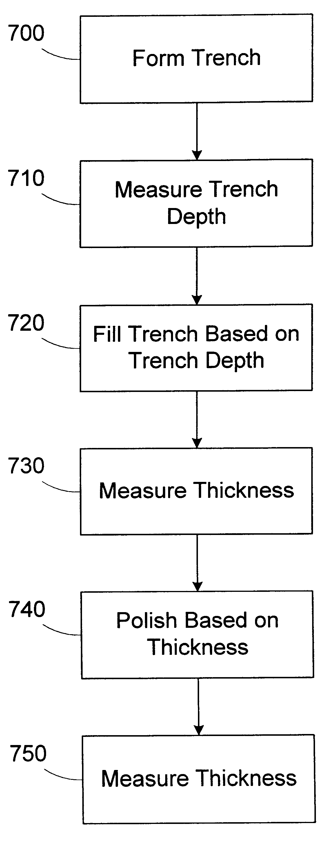
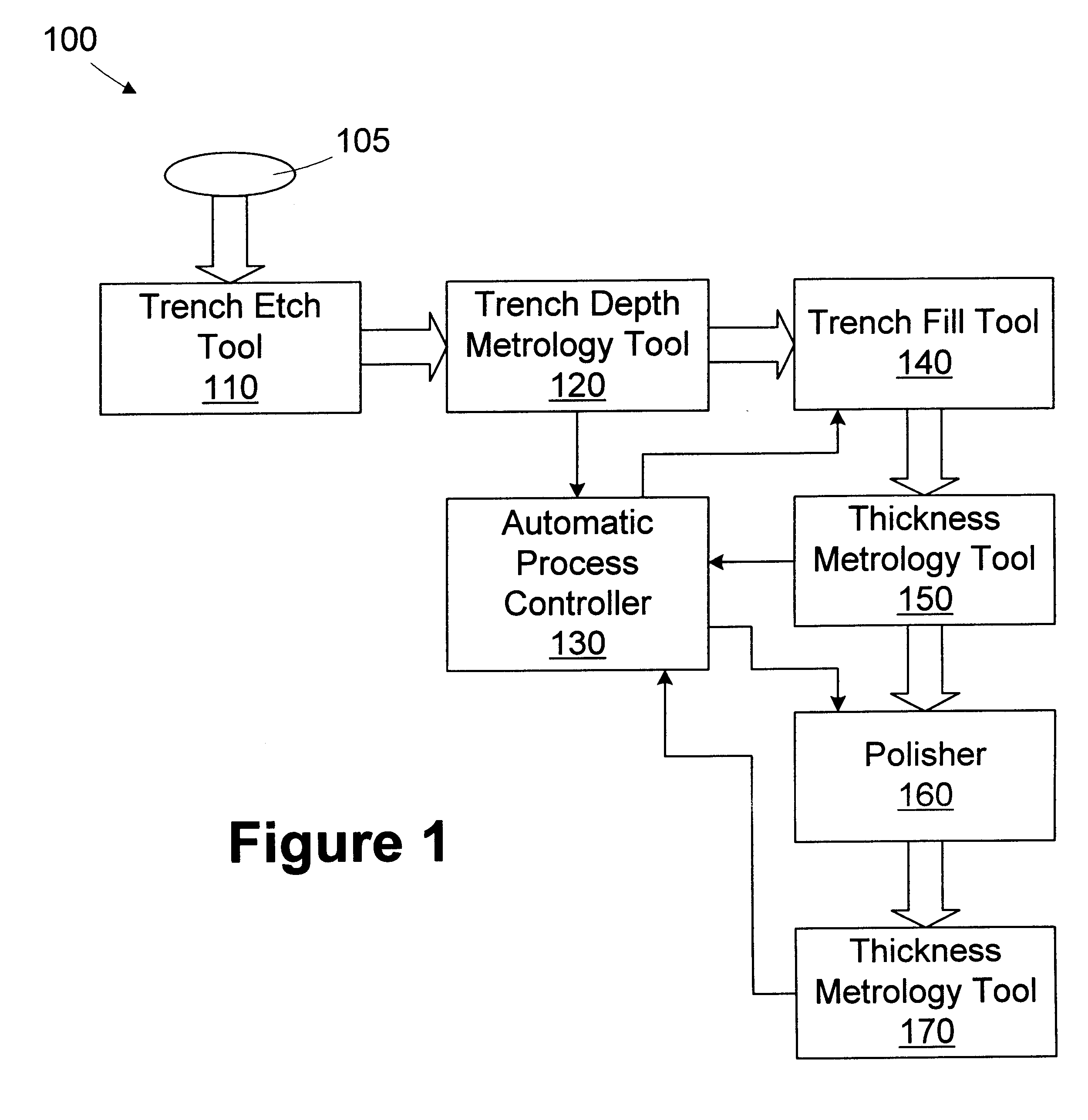
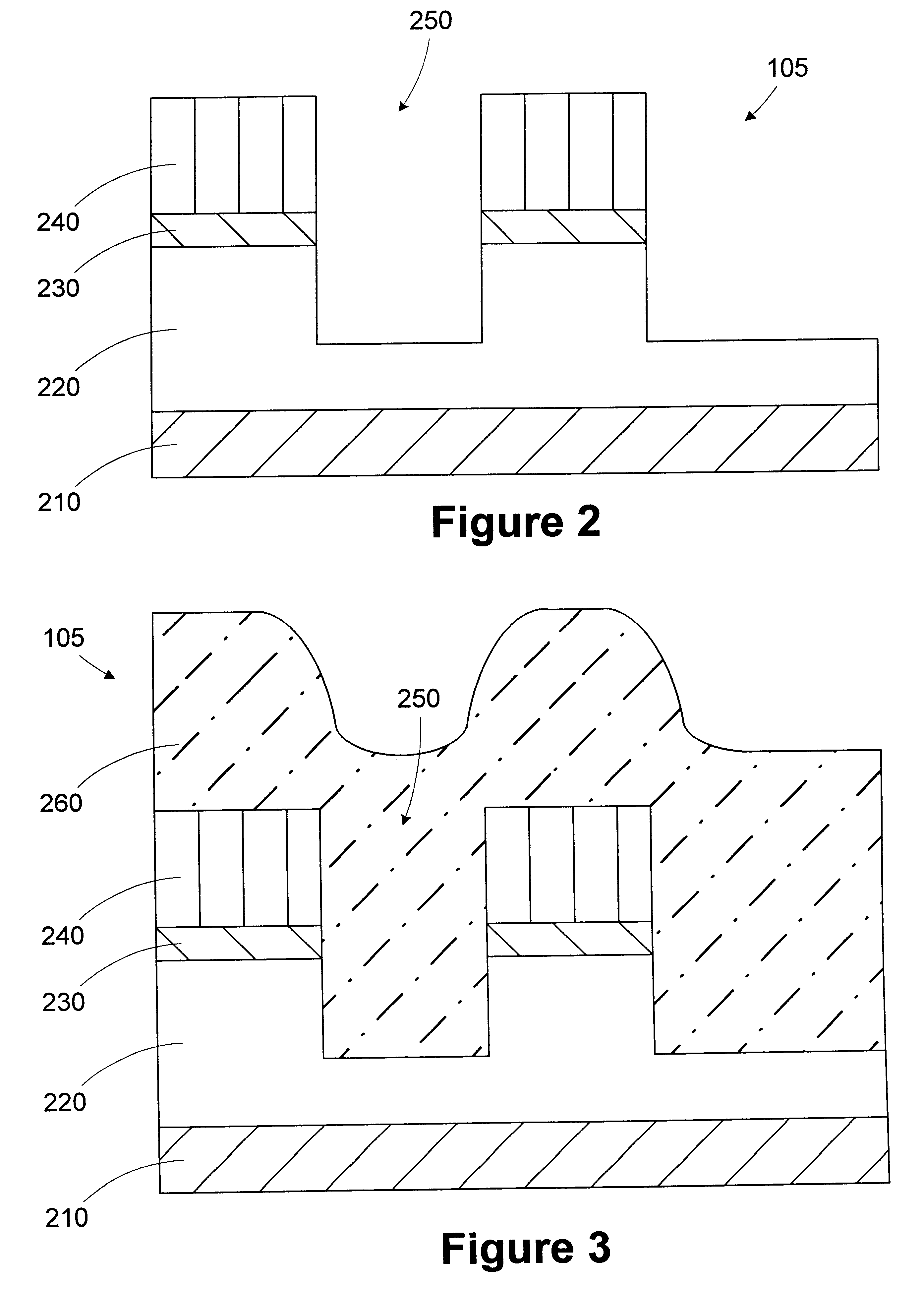
Referring now to the Figures, and particularly to FIG. 1, a simplified block diagram of a processing line 100 useful for forming a trench feature in a wafer 105 is provided. The operation of the processing line 100 of FIG. 1 is described in reference to the cross-section views of the w...


PUM


Abstract

A method for filling a trench is provided. A wafer having at least a first layer formed thereon is provided. A trench is formed in the first layer. The depth of the trench is measured. A target thickness is determined based on the depth of the trench. A second layer of the target thickness is formed over the trench. A processing line includes a trench etch tool, a first metrology tool, a trench fill tool, and an automatic process controller. The trench etch tool is adapted to form a trench in a first layer on a wafer. The first metrology tool is adapted to measure the depth of the trench. The trench fill tool is adapted to form a second layer over the first layer based on an operating recipe. An automatic process controller is adapted to determine a target thickness based on the depth of the trench and modify the operating recipe of the trench fill tool based on the target thickness.

Description

1. Field of the InventionThis invention relates generally to semiconductor manufacturing, and, more particularly, to a method for filling trenches.2. Description of the Related ArtA conventional integrated circuit device, such as a microprocessor, is typically comprised of many thousands of semiconductor devices, e.g, transistors, formed above the surface of a semiconductive substrate. For the integrated circuit device to function, the transistors must be electrically connected to one another through conductive interconnections. Many modem integrated circuit devices are very densely packed, i.e., there is very little space between the transistors formed above the substrate. Thus, these conductive interconnections must be made in multiple layers to conserve plot space on the semiconductive substrate. One technique for interconnecting devices on the same plane is to form a trench in an insulative layer (e.g., silicon dioxide or silicon nitride) and fill the trench with a conductive ma...

Claims


Application Information

Patent Timeline
Patent Type & Authority Patents(United States)
IPC IPC(8): H01L21/762H01L21/70H01L21/66
CPCH01L22/20H01L21/76229
Inventor CAMPBELL, WILLIAM J.FULFORD, H. JIMRAEDER, CHRISTOPHER H.CHRISTIAN, CRAIG W.SONDERMAN, THOMAS
Owner GLOBALFOUNDRIES INC
Why Eureka
Try Eureka