

Method for transferring semiconductor device layers to different substrates
- Summary
- Abstract
- Description
- Claims
- Application Information
AI Technical Summary
Benefits of technology
Problems solved by technology
Method used
Image

Examples
Embodiment Construction
1. The Preferred Embodiment.
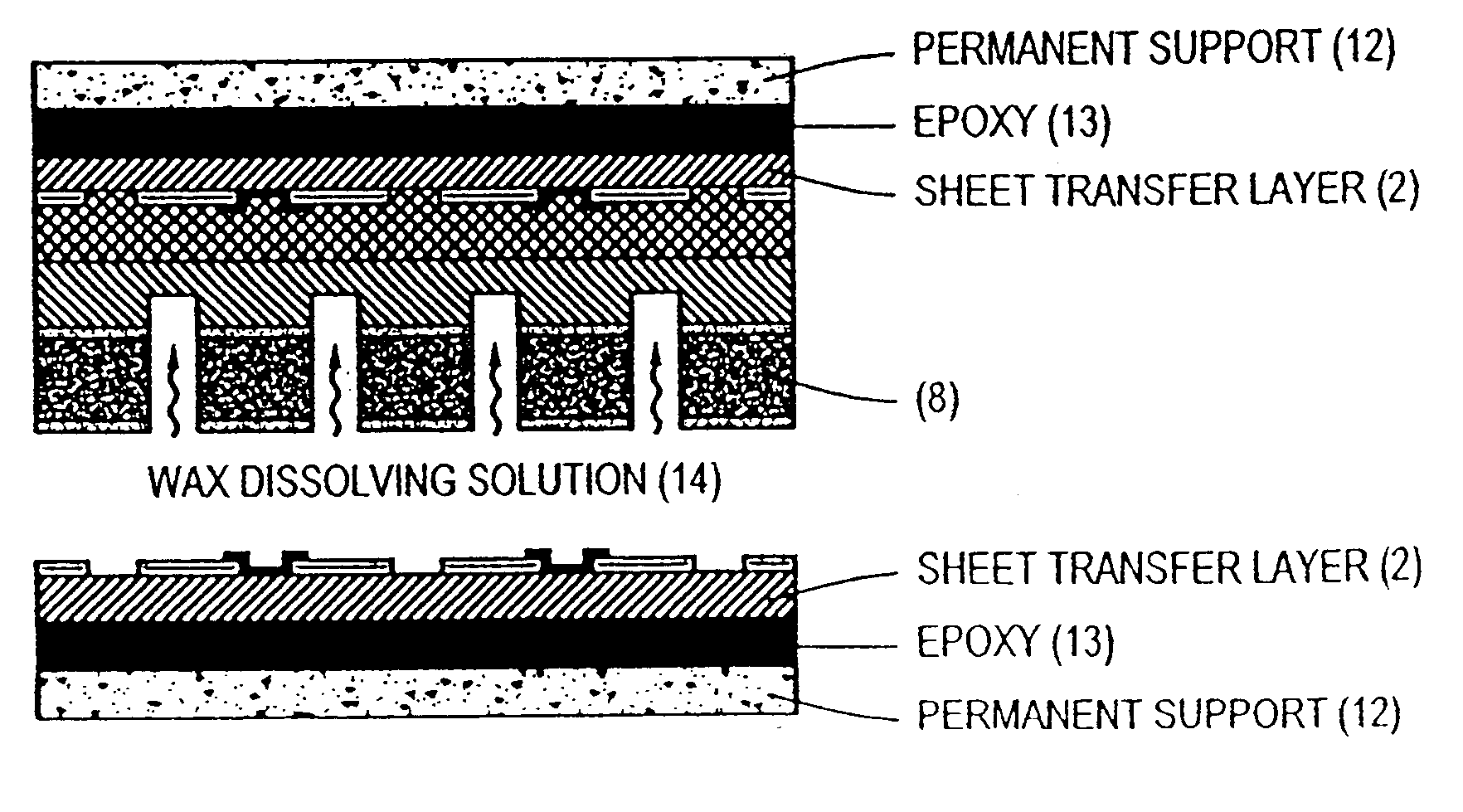
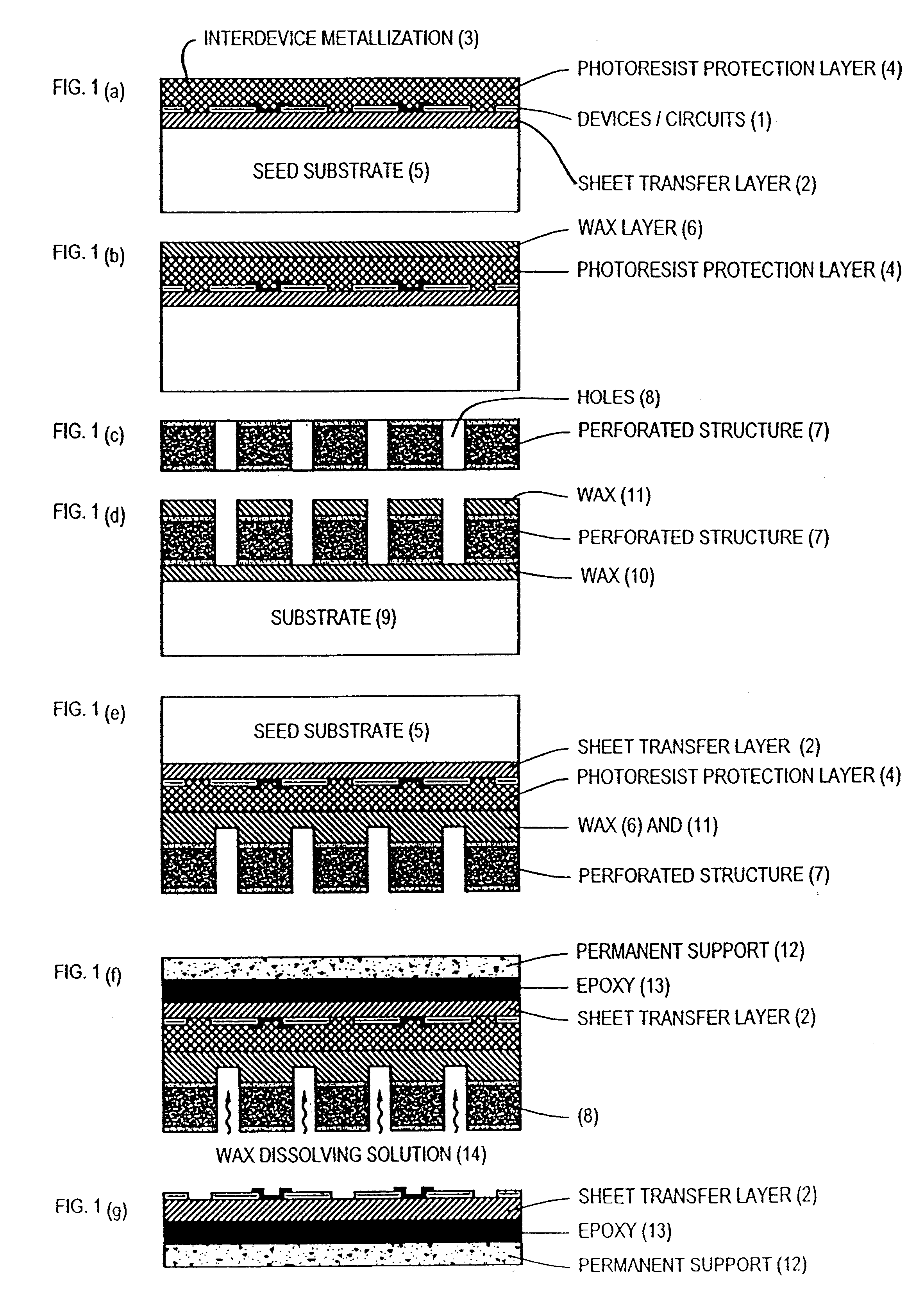
As shown by FIG. 1(a), the initial preferred step of this method is the fabrication of semiconducting devices and / or circuits 1 on a thin active layer (sheet transfer layer 2) including, if desired, interconnection metallization 3 between the devices and / or circuits, as appropriate.
Examples of the semiconducting devices and / or circuits 1 fabricated into the active layer 2 include, but are not limited to, active matrix circuitry for displays and a matrix of radiation sensing elements. Other semiconducting devices and / or circuits, including passive devices, can be also used.
Interconnection metallization 3 comprises preferably gold, or aluminum or other metal compatible with the particular semiconducting devices and / or circuits 2 used. The choice of a particular metal for interconnection metallization 3 is made according to general principles of the art of fabrication of the semiconducting devices and / or circuits 2 known to those reasonably skilled in the ar...
PUM
 Abstract
Description
Claims
Application Information