
Method for measuring collector and emitter breakdown voltage of bipolar transistor

Inactive Publication Date: 2001-09-18
NEC ELECTRONICS CORP
View PDF3 Cites 11 Cited by
  • Summary
  • Abstract
  • Description
  • Claims
  • Application Information

AI Technical Summary

Problems solved by technology

For this reason, it is apparent that the above-mentioned prior art has not taken sufficient countermeasures to cause no destroy of the device and to accurately perform measurement.
Therefore, an emitter and base breakdown voltage (zener breakdown) cannot be accurately defined.
Therefore, there has been another problem in that characteristics other than the punch through breakdown voltage cannot be defined in respect of the reliability and integration degree of the device characteristics.
Furthermore, the prior art has a problem in that a device area cannot be reduced because the diode element is provided in addition to the bipolar element.
In consideration of adaptation to an increase in the fineness and performance of the device, moreover, the following problem arises.
Therefore, the reverse junction leakage current of the diode is increased so that the function of the diode cannot be performed.
In this case, when the current of 100 .mu.A is instantaneously caused to flow, there is a particular possibility that the base and emitter junction might destroy.
For this reason, the above-mentioned prior art has had a problem in that a measuring time is increased and a throughput is deteriorated.

Method used


Image

  • Method for measuring collector and emitter breakdown voltage of bipolar transistor
  • Method for measuring collector and emitter breakdown voltage of bipolar transistor
  • Method for measuring collector and emitter breakdown voltage of bipolar transistor

Examples


Embodiment Construction

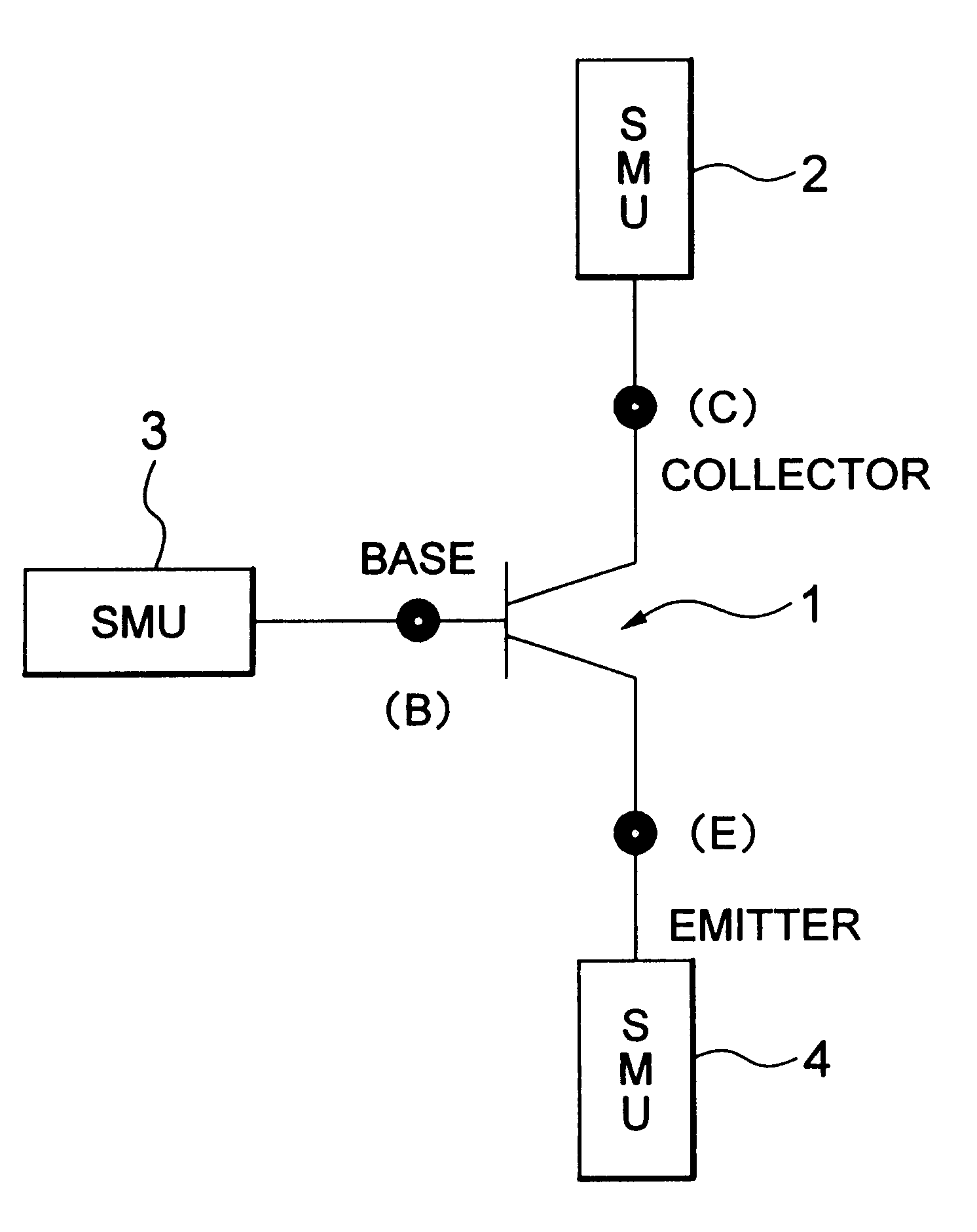
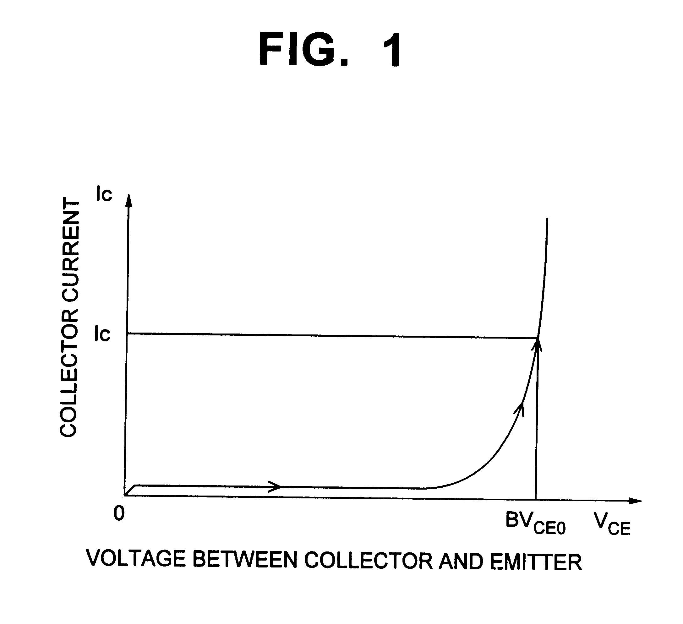
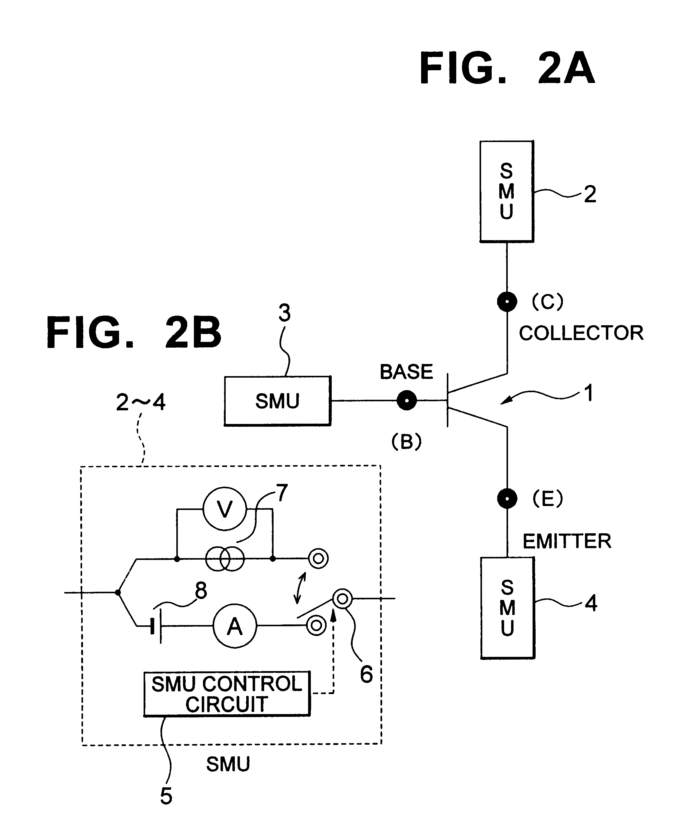
An embodiment of the present invention will be specifically described below with reference to the accompanying drawings. FIG. 1 is a graph showing the relationship between a collector and emitter voltage VCE and collector current IC according to a method of the embodiment of the present invention, FIG. 2A is a diagram showing the connecting state of each terminal of a vertical bipolar transistor and a measuring unit (SMU), FIG. 2B is a circuit diagram showing the structure of the measuring unit, FIG. 3 is a typical view showing a measuring method, and FIG. 4 is a sectional view showing the structure of a vertical NPN bipolar transistor which is a measuring object.

As shown in FIG. 2A, measuring units (SMU) 2, 3 and 4 acting as measuring equipment are connected to a collector (C), a base (B) and an emitter (E) of a device 1 whose characteristic is to be measured, respectively. As shown in FIG. 2B, the measuring units 2 to 4 have a switch 6 for switching the connection of a current sou...


PUM


Abstract

A collector current and a ratio of current amplification which are to measure a punch through breakdown voltage (BVCEO) of a vertical bipolar transistor device are indicated as IC and hFE. A base current IB having 1% of IC / hFE or less is caused to flow to a base of the device. In the state in which the base current IB is injected into a base terminal, a constant voltage (VE) of a ground potential is applied to an emitter terminal and a voltage sweep is performed with a predetermined step width over a collector terminal. When the collector current reaches the current IC to measure the punch through breakdown voltage, the voltage sweep is stopped to measure the punch through breakdown voltage as a collector voltage VC. Consequently, a collector and emitter punch through breakdown voltage of the bipolar device can be accurately measured, and furthermore, the device can be prevented from breaking down when measuring the punch through breakdown voltage.

Description

1. Field of the InventionThe present invention relates to a breakdown voltage characteristic of a vertical bipolar device, and more particularly to a method for measuring a collector and emitter breakdown voltage of a bipolar transistor which can measure a punch through breakdown voltage characteristic between a collector and an emitter with high accuracy.2. Prior ArtIn a vertical bipolar device, a manufacturing margin for the depth of each junction of a collector, a base and an emitter has been strictly restricted with an increase in fineness and performance of the device, and it is one of important factors that a breakdown voltage characteristic between electrodes, particularly, a punch through breakdown voltage characteristic between the collector and the emitter should be accurately defined ("Very High Digital Device Series 1, Very High Bipolar Device", Chapter 2, section 3-5 (pages 56 to 60) by Baifukan, the first edition was issued on Nov. 15, 1985).For this reason, usually, a...

Claims


Application Information

Patent Timeline
IPC IPC(8): G01R31/26H01L21/331H01L21/66H01L29/73H01L29/732
CPCG01R31/261
Inventor WAKABAYASHI, MASARU
Owner NEC ELECTRONICS CORP
Learn More