Wiring design apparatus, wiring determination apparatus and methods thereof

a technology of wiring determination and wiring design, which is applied in the direction of computation using non-denominational number representation, program control, instruments, etc., can solve the problems of unnecessarily dense wire density among the pins, inability to detect such illegal wiring, and repetition of work taking a long tim

Inactive Publication Date: 2001-09-25
IBM CORP
View PDF0 Cites 153 Cited by
  • Summary
  • Abstract
  • Description
  • Claims
  • Application Information

AI Technical Summary

Benefits of technology

As described in the above, according to the wiring design apparatus, the wiring determination apparatus and the methods thereof, it can be quickly determined whether or not the wiring is 100% feasible (wiring solution exists) in wiring a printed circuit, etc., before all the wiring design is completed.Also, according to the wiring design apparatus, the wiring determination apparatus and the methods thereof, an illegal wiring in which a route detours largely or turns around a pin can be quickly and efficiently detected and corrected before all the wiring design is completed in designing wiring in a specific area, particularly in wiring a semiconductor package, etc.Also, according to the wiring design apparatus, the wiring determination apparatus and the methods thereof, a wiring solution can be quickly and efficiently obtained to detect and correct an illegal wiring in designing a wiring resulting in a large reduction of the labor of the worker.Also, according to the wiring design apparatus, the wiring determination apparatus and the methods thereof, Delaunay triangulation can be utilized in designing a wiring to quickly and efficiently obtain an optimum wiring solution.While the present invention has been particularly described, in conjunction with a specific preferred embodiment, it is evident that many alternatives, modifications and variations will be apparent to those skilled in the art in light of the foregoing description. It is therefore contemplated that the appended claims will embrace any such alternatives, modifications and variations as falling within the true scope and spirit of the present invention.

Problems solved by technology

An improvement of wiring route and design speed has been disclosed, however, it is not determined until the wiring design has been completed whether or not wiring of a printed circuit and the like is 100% possible (whether or not a wiring solution exists) in the prior art wiring design apparatus.
In designing wiring in a specific area such as a wiring of a semiconductor package, an illegal wiring in which the wire density among the pins is unnecessarily dense and the route detours excessively, or turns round the periphery of pins has to be detected and corrected even if there is a wiring solution.
However, prior to this invention it was not possible to detect such illegal wiring until the wiring design had been completed in the prior art wiring design apparatus.
Such repetition of work took a very long time and it is a heavy burden on the designer.
No wiring determination apparatus has ever existed so far which uses Delaunay triangulation method in wiring design to quickly determine presence or absence of wiring solution for detecting and correcting an illegal wiring.

Method used


Image

  • Wiring design apparatus, wiring determination apparatus and methods thereof
  • Wiring design apparatus, wiring determination apparatus and methods thereof
  • Wiring design apparatus, wiring determination apparatus and methods thereof

Examples


first embodiment

A first embodiment of this invention is now described hereunder.

While this invention is described hereunder taking an application of this invention to wiring a semiconductor package as an example, this invention may be also applicable to a wide use including a design of a printed circuit, etc.

Computer Network 1

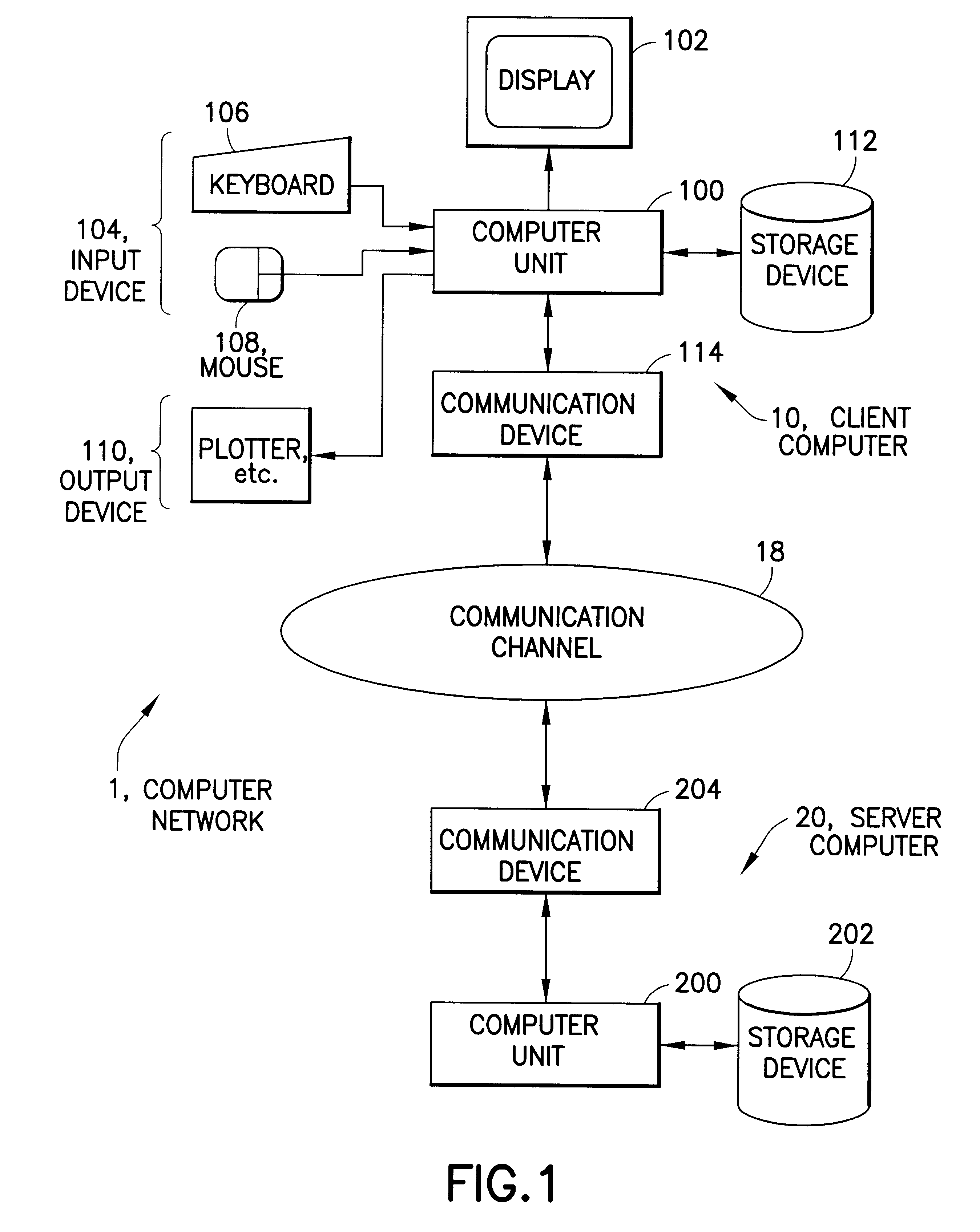
A computer network 1 to which the wiring design method and the wiring determination method of this invention are applied is described hereunder.

FIG. 1 is a diagram showing an example of the configuration of the computer network to which this invention is adapted.

As shown in FIG. 1, the computer network 1 comprises n client computers 10, a communication channel 18 and a server computer 20 (FIG. 1 shows an example where n=1).

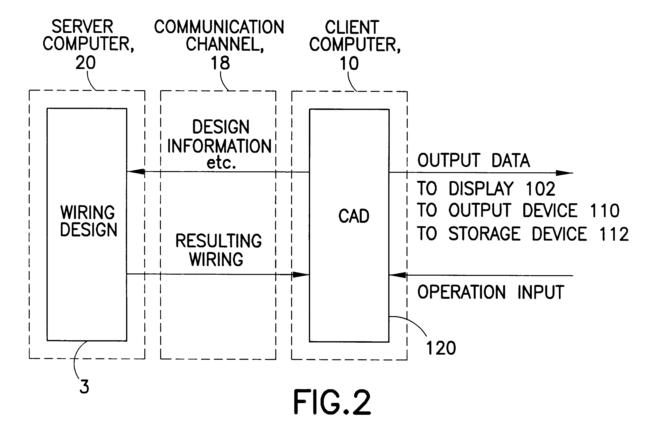
FIG. 2 is a diagram showing an allotment of function between the client computer 10 and the server computer 20.

As shown in FIG. 2, the client computer 10 executes a CAD (computer aided design) software 120 for effecting a design of a semiconductor chip while...

second embodiment

The second embodiment of this invention is now described hereunder.

As described in the first embodiment, the wiring design method of this invention determines that a triangulated edge having identification numbers (STATIC_ID) p, q assigned to the pins at the ends crosses a wiring connecting to a pin r (p

FIG. 25 is a diagram showing an example of a re-entrant portion of a semiconductor package.

On the other hand, when identification numbers 0 to 100 are assigned to 101 pins of the semiconductor package, a re-entrant portion is in advent in which a portion assigned an identification number first is adjacent to a portion assigned an identification number last, specifically, a portion in which pins assigned identification numbers STATIC_ID_0, 1, 2 and pins assigned identification numbers STATIC_ID_97, 98, 100 share a triangulated edge.

The wiring design method given as the first embodiment can not be applied as it is to such re-entrant portion in which a pin...

third embodiment

The Third Embodiment

The third embodiment of this invention is now described hereunder.

In the third embodiment, a method of detecting a wiring in which a redundancy (illegality) such as detouring occurs as a result of the wiring design method of this invention as described in the first and the second embodiments.

FIG. 28 is a flow chart showing a process (S140) in which the wiring design software 3 detects a redundant (illegal) wiring such as detouring wiring.

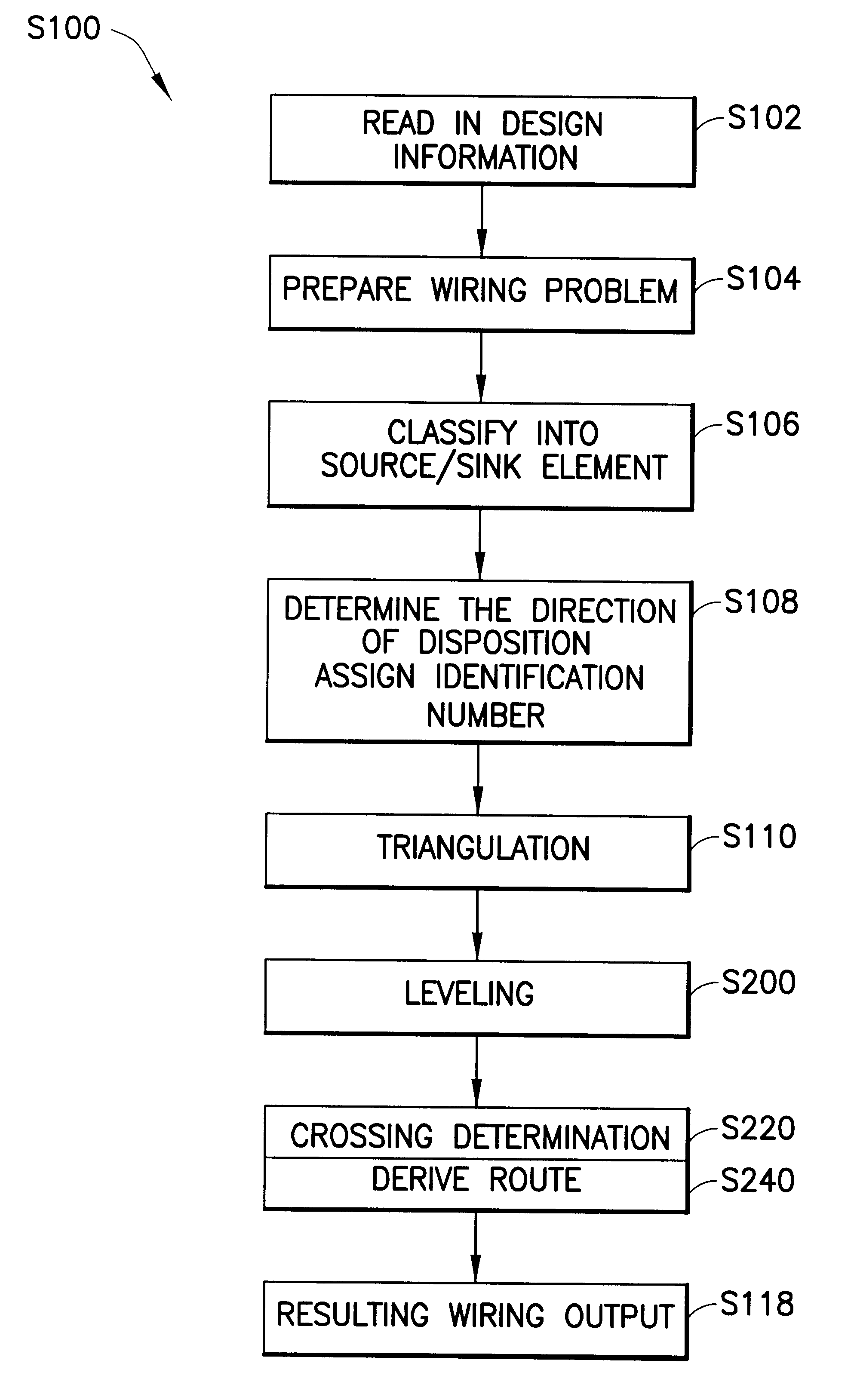
As shown in FIG. 28, in step 142 (S142), the wiring design software 3 effects the processes of reading design information, preparing a wiring problem and classifying binding pads and pins into source and sink elements in the manner similar to the process of S102 to S106 shown in FIG. 3.

In step 144 (S144), the wiring design software 3 effects the triangulation process in the manner similar to the process of S110 shown in FIG. 3.

In step 200 (S200), the wiring design software 3 effects the leveling process in the manner similar to t...


PUM


Abstract

The present invention relates generally to effectively design a wiring of a semiconductor package, etc., in a short time. A wiring design software (SW) reads in design information indicating disposition of pads on a chip, disposition of pins on a package, and relationship of correspondence between the pads and the pins, analyzes it to prepare a wiring problem, classifies the pads and the pins into source and sink elements, and assigns consecutive identification numbers to the pads and the pins with a same identification number being assigned to a pad and a pin which are connected each other (S102, . . . , S108). The wiring design SW generates a virtual triangle having a source / sink element as an apex by applying Delaunay triangulation to the source and the sink elements (S110). The wiring design SW level classifies the pins using the generated triangle (S200). The wiring design SW determines whether or not an edge of the triangle crosses a wiring and connects the edges which are determined to cross each other to derive a route of wiring (S220), outputting the result of wiring design (S118).

Description

The present invention relates to a wiring design apparatus, wiring determination apparatus and methods thereof for designing an optimum wiring routine between bonding pads provided on a semiconductor chip and pins (terminals) provided on a semiconductor package.A wiring design apparatus which automatically or semi-automatically designs a wiring of a printed circuit substrate or a wiring between bonding pads of a semiconductor chip and pins (terminals) of a semiconductor package which is used in a electronic equipment is disclosed in PUPA 5-143689. An improvement of wiring route and design speed has been disclosed, however, it is not determined until the wiring design has been completed whether or not wiring of a printed circuit and the like is 100% possible (whether or not a wiring solution exists) in the prior art wiring design apparatus.In designing wiring in a specific area such as a wiring of a semiconductor package, an illegal wiring in which the wire density among the pins is ...

Claims


Application Information

Patent Timeline
Patent Type & Authority Patents(United States)
IPC IPC(8): G06F17/50
CPCG06F17/5077G06F30/394
Inventor MATSUMOTO, HIROYUKI
Owner IBM CORP
Why Eureka
Try Eureka