
Reading device for integrated circuit memory

Inactive Publication Date: 2001-10-23
STMICROELECTRONICS SRL
View PDF8 Cites 44 Cited by
  • Summary
  • Abstract
  • Description
  • Claims
  • Application Information

AI Technical Summary

Benefits of technology

It is an object of the present invention to reduce the read access time of memories, namely the time in which the data reflecting the state stored in one or more memory cells becomes available at an output. In one example, a maximum read access time of 25 nanoseconds may be provided instead of the typical prior art time of 80 nanoseconds.

Problems solved by technology

This absorption of current produces a great variation of voltage in the signal applied at the input to the differential amplifier, causing it to switch over.
This slows down the setting up of the real data at the output.
In practice, the sequencing operations needed to start up the various circuits of the reading device and the parasitic oscillations of the amplifier lengthen the read access time.

Method used


Image

  • Reading device for integrated circuit memory
  • Reading device for integrated circuit memory
  • Reading device for integrated circuit memory

Examples


Embodiment Construction

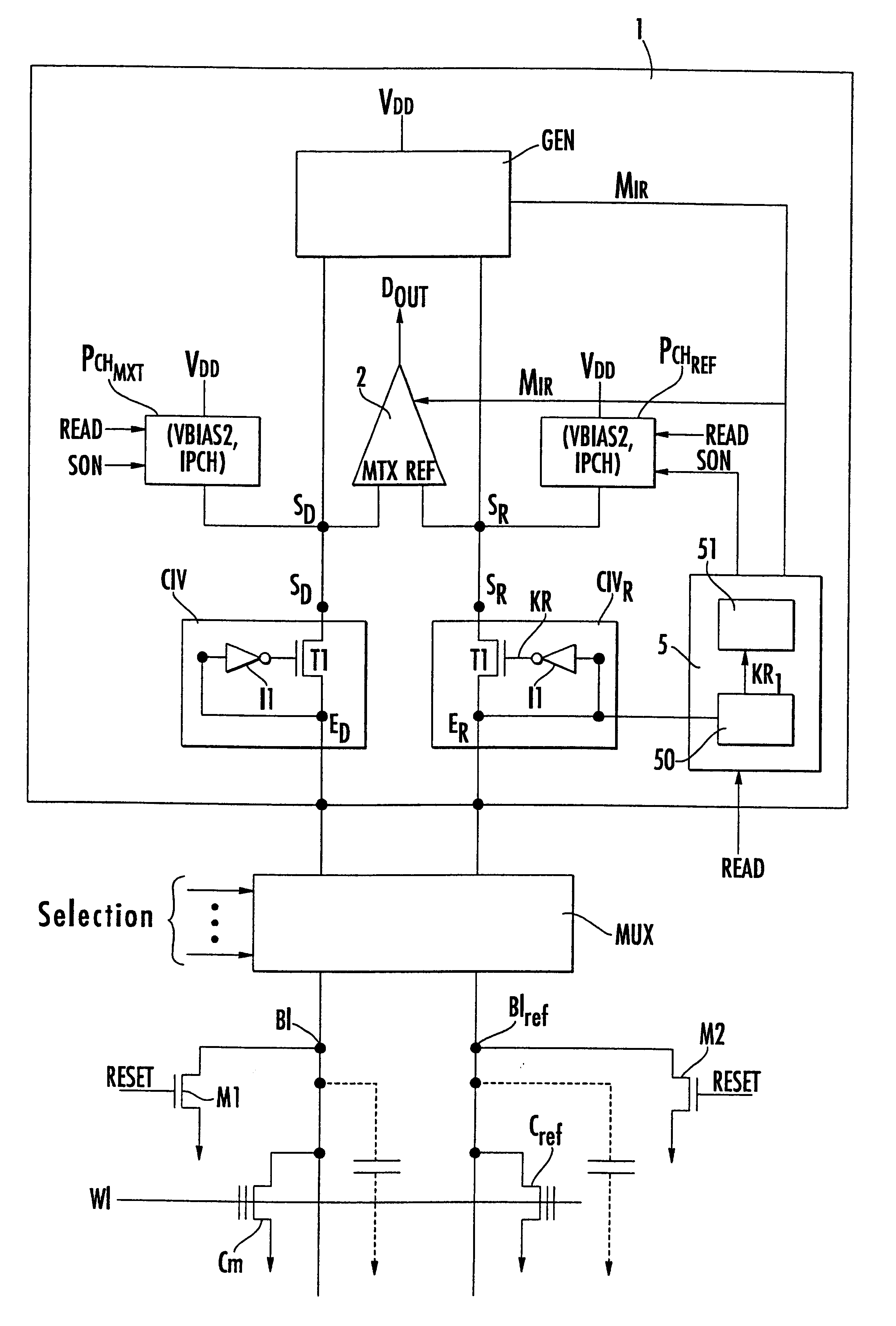
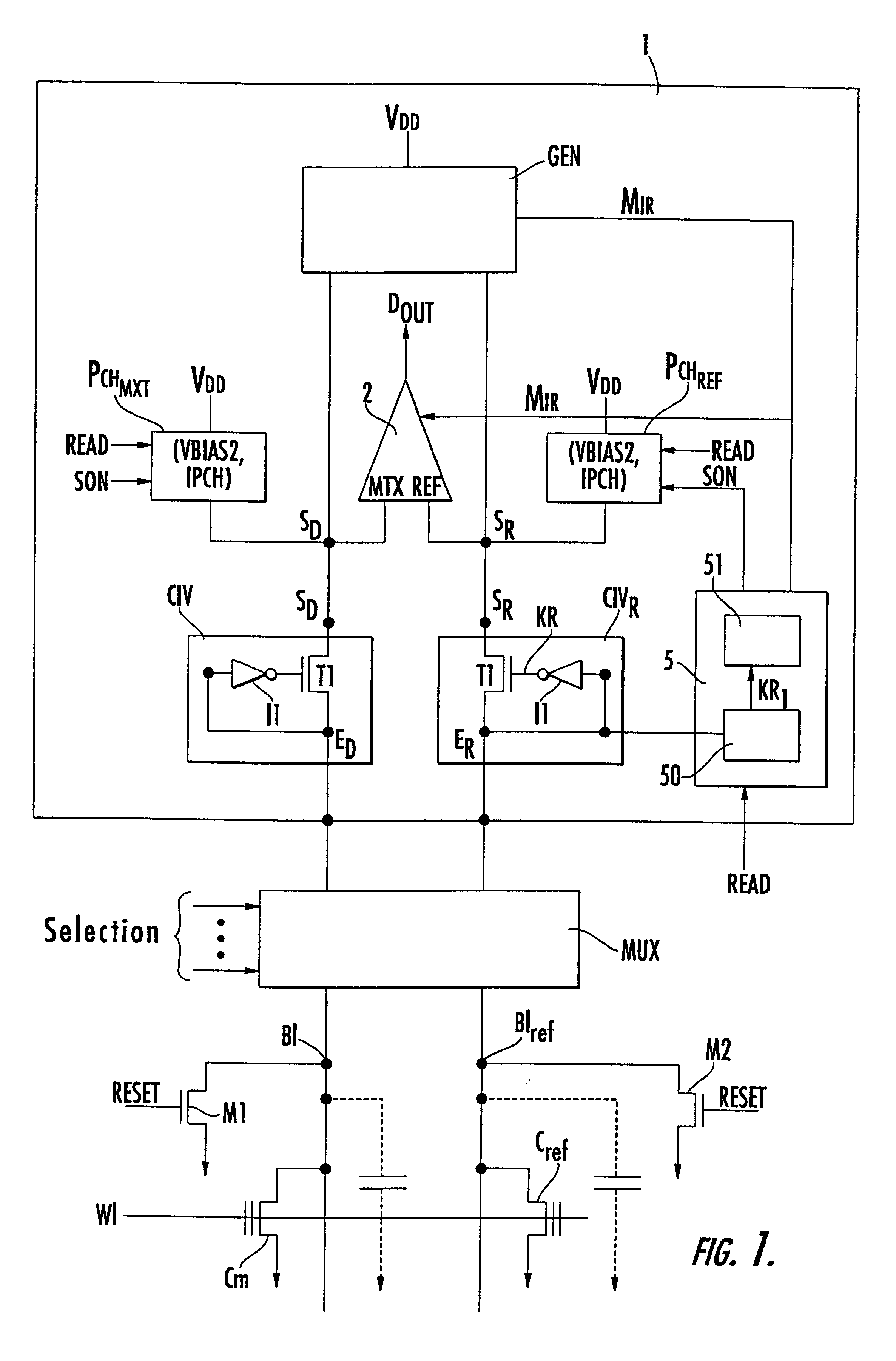
FIG. 1 is a block diagram of a reading device according to the present invention for reading cells of a memory. In the illustrated example, the memory is an EPROM type memory. A cell of this memory includes a floating-gate transistor having its drain connected to a bit line of the memory array and its gate connected to a word line. The reference cell or cells are generally located on a reference bit line at the end of the memory array.

The complexity of the architecture of the memory may vary. The architecture may or may not include access transistors. It may include a grouping of bit lines or other lines, and the memory may be of some other type (e.g. non-volatile, etc.). The invention thus applies to numerous types and architectures of memories.

A data bit line B1 and a reference bit line Bl.sub.ref of the memory may be seen in FIG. 1. A memory cell Cm for the data bit line and a memory cell C.sub.ref for the reference bit line is also included. In the example, these cells are forme...


PUM


Abstract

A device for reading a memory including precharging circuits for precharging the inputs of a differential amplifier to a precharging voltage. The precharging voltage may be at an intermediate voltage level between a precharging voltage level of the bit lines and the voltage level of the logic supply voltage. This provides for a very fast build-up, during a following evaluation phase, of the output of the amplifier in a state corresponding to that of the cell being read. An internal detection circuit may also be included to detect an end of the precharging to stop the precharging circuit and activate the read current generator for the evaluation phase.

Description

FIELD OF THE INVENTIONThe present invention relates to the field of electronic circuits, and, more particularly, to reading devices for integrated circuit memories. The present invention may be applied especially, but not exclusively, to erasable programmable read only memories (EPROMs) or one-time-programmable (OTP) type non-volatile electrically programmable memories.BACKGROUND OF THE INVENTIONThe cells of a memory are usually organized in matrix form with bit lines and word lines. The bit lines are the conductors through which the state stored in a cell is read. Thus, when a memory cell is addressed in read mode, the corresponding word line is selected and the corresponding bit line is connected to a read device.In general, it is not just one but several memory cells that are read when a memory word is read. The cells forming a memory word typically belong to the same word line, and a respective bit line corresponds to each cell. In read mode, each one of these bit lines is conne...

Claims


Application Information

Patent Timeline
IPC IPC(8): G11C7/00G11C7/12G11C16/24G11C16/28G11C16/06G11C7/08
CPCG11C7/12G11C16/24G11C16/28
Inventor FOURNEL, RICHARDVARISCO, LAURA
Owner STMICROELECTRONICS SRL
Learn More