
Precharge arrangement for read access for integrated nonvolatile memories

a nonvolatile memory and precharge arrangement technology, applied in static storage, digital storage, instruments, etc., can solve the problems of specific time loss, long read access time of memory cells, and the need to start the operation of precharging the bit line, so as to reduce the read access time

Active Publication Date: 2007-06-26
INFINEON TECH AG
View PDF5 Cites 9 Cited by
  • Summary
  • Abstract
  • Description
  • Claims
  • Application Information

AI Technical Summary

Benefits of technology

[0008]The object of the present invention is to reduce the read access times in nonvolatile memories, to eliminate the abovementioned disadvantages and to afford further advantages.
[0011]In a first embodiment according to the invention, in a minimal configuration, it is provided that the bit line is directly connected to the sense amplifier and thus still continuously has the precharge potential thereof applied to it. For this purpose, the source line is isolated from the ground potential via a ground switching element as long as the bit line is not selected, that is to say the source line is “floating”. This advantageously prevents the bit line from being discharged in the case of a conductive memory cell.
[0012]In a further embodiment, it is provided that the bit line is connected to a precharge potential via a first controllable switching element. In an advantageous manner, the source line is also connected to the precharge potential by means of a second controllable switching element. The latter has the advantage that there is no need to effect any charge reversal operations from the bit line to the source line via a conductive memory cell. A third controllable switching element is inserted between the source line and the ground potential. These three controllable switching elements are preferably transistors whose control inputs are connected to one another and are at a potential that is present at the output of an inverter in a manner dependent on the address selection signal present at the input of the inverter.
[0014]This precharge arrangement has the advantage that it does not require an external precharge signal. At the same time, any signal processing steps for such a signal are advantageously obviated. Furthermore, it is advantageous that the precharge arrangement according to the invention is realized with a very small number of components which, in a preferred embodiment, can be concomitantly introduced simultaneously on the memory chip.
[0015]It is furthermore advantageous that the voltage of the precharge potential that is continuously applied to the bit line and the source line during the deselected state of the bit line has the same magnitude as the operating voltage of the sense amplifier. Consequently, there are advantageously no time losses during the read access of the sense amplifier since, on the one hand, the latter no longer has to charge any parasitic capacitances and, on the other hand, the bit line is already at the operating voltage of the sense amplifier.
[0017]This affords the advantage that the operating point is reached significantly more rapidly and the access time decreases. This is of great significance owing to the rising clock frequency and smaller feature size and thus larger time constants in the future.

Problems solved by technology

This results in a correspondingly long read access time of the memory cell.
In this case, what has proved to be disadvantageous is that the operation of precharging the bit line has to be started at a specific point in time prior to the read-out.
Fast sense amplifiers are regulating devices which reach their operating point relatively slowly in the case of a large change in potential, thereby resulting in specific time losses.

Method used


Image

  • Precharge arrangement for read access for integrated nonvolatile memories
  • Precharge arrangement for read access for integrated nonvolatile memories
  • Precharge arrangement for read access for integrated nonvolatile memories

Examples


Embodiment Construction

[0024]Identical elements having identical functions are provided with the same reference symbols.

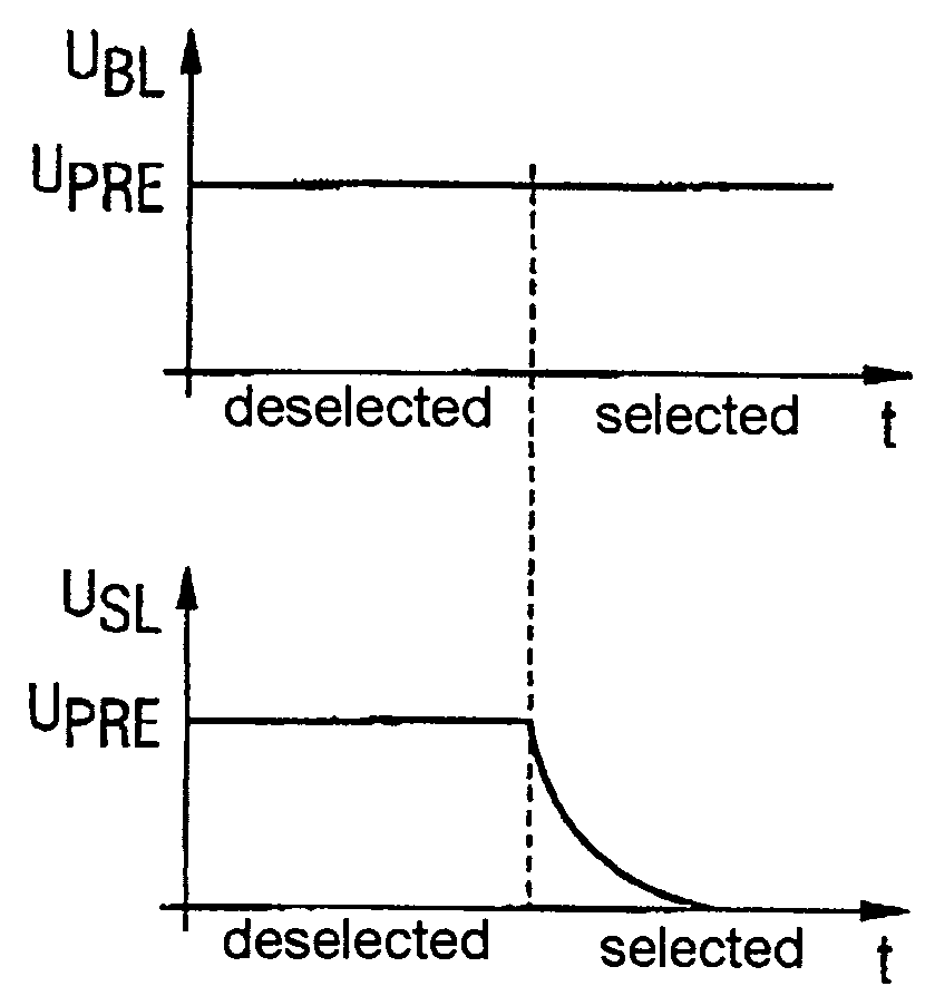
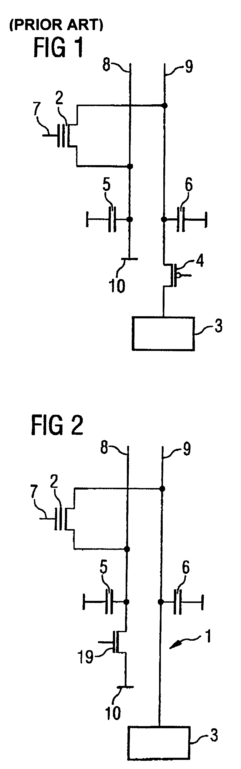
[0025]FIG. 1 schematically illustrates a read access arrangement according to the prior art. One terminal of the memory cell 2 is connected to a source line 8, and a further terminal is connected to a bit line 9. The parallel illustration of the source line 8 and the bit line 9 is purely schematic. In practice, these lines may be arranged in different ways.

[0026]The source line 8 is connected to a fixed ground potential 10 by one of its ends. The bit line 9 is coupled to a sense amplifier 3 via an address switching element 4.

[0027]Parasitic capacitances of the lines 8, 9 are respectively illustrated as a parasitic capacitance 5 of the source line 8 and as a parasitic capacitance 6 of the bit line 9.

[0028]If the memory cell 2 is conductive, then it connects the bit line 9 to the ground potential 10 via the source line 8, the bit line 9 with its parasitic capacitance 6 being discharged, th...


PUM


Abstract

Precharge arrangement for read access for integrated nonvolatile memories having at least one memory cell (2), at least one source line (8), at least one bit line (9), at least one sense amplifier (3) and at least one precharge potential, the bit line (9) continuously having the precharge potential in a deselected state of the bit line (9), and the source line (8) having a predetermined reference potential, in particular a ground potential (10), in a selected state of the bit line (9).

Description

TECHNICAL FIELD[0001]The invention relates to a precharge arrangement in accordance with the preamble of claim 1 for read access for integrated nonvolatile memories having at least one memory cell, at least one source line, at least one bit line, at least one sense amplifier and a precharge potential.BACKGROUND ART[0002]In the case of nonvolatile memories (EEPROM, flash, EPROM, OTP, . . . ), one terminal of the memory cell is always at a fixed potential, for example ground potential. This line is the so-called source line. The other terminal of the memory cell is connected to the so-called bit line. The memory cell is read via the bit line.[0003]If the bit line is not active, that is to say if a read-out operation is not being effected, then the bit line, to which a precharge potential is applied from the previous read-out operation, can be discharged via a conductive memory cell since the memory cell is connected by its other terminal to the source line carrying ground potential.[0...

Claims


Application Information

Patent Timeline
Patent Type & Authority Patents(United States)
IPC IPC(8): G11C16/00G11C7/06G11C16/24G11C16/26
CPCG11C7/06G11C16/24G11C16/26
Inventor DEML, CHRISTOPHLIEBERMANN, THOMASPAPARISTO, EDVINROGL, STEPHAN
Owner INFINEON TECH AG
Learn More