Liquid crystal display device

a display device and liquid crystal technology, applied in logic circuit coupling/interface arrangement, amplifiers with impedence circuits, instruments, etc., can solve the problems of large variations difficulty in integrally forming liquid crystal panels and driver circuits thereof with polysilicon, and difficulty in forming voltage follower circuits with polysilicon, etc., to achieve sufficient reduction of the variation in output potential between the circuits, the effect of large variation in characteristics and precise offset cancelling

Inactive Publication Date: 2001-11-06
SONY CORP
View PDF21 Cites 118 Cited by
  • Summary
  • Abstract
  • Description
  • Claims
  • Application Information

AI Technical Summary

Benefits of technology

The liquid crystal display device of the present invention employs a source follower circuit of the above configuration as an output buffer for driving each column line. Highly precise offset cancelling can therefore be carried out with this source follower circuit even with circuits made of transistors such as polysilicon TFTs having a large threshold voltage Vth and having large amounts of variation in characteristics. Variations in output potential between each circuit can therefore be sufficiently reduced even when a plurality of circuits are lined up in parallel.

Problems solved by technology

However, in integrally forming a liquid crystal panel and a driver circuit thereof using polysilicon, complicated circuits for the operational amplifiers and variation in characteristics and large threshold voltage Vth of polysilicon TFTs make it difficult to form voltage follower circuits with polysilicon.
This causes difficulty in integrally forming a liquid crystal panel and a driver circuit thereof with polysilicon.
Therefore, when this circuit is used as an output buffer for charging each column line capacitor, there are large variations in output potential between the circuits.
It is therefore difficult to employ a source follower circuit of the current configuration as an output buffer as it is for an integration of a liquid crystal panel and a driver using polysilicon.

Method used


Image

  • Liquid crystal display device
  • Liquid crystal display device
  • Liquid crystal display device

Examples


first embodiment

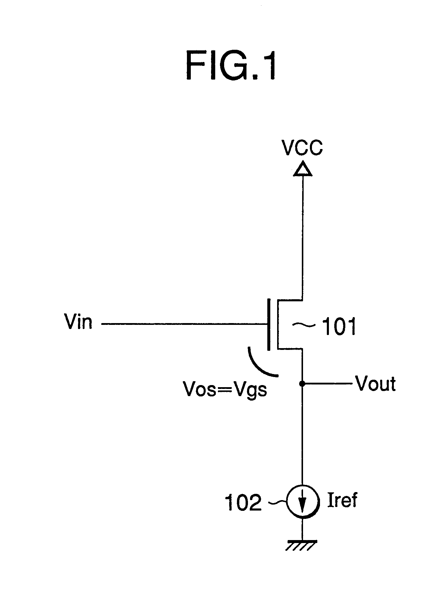
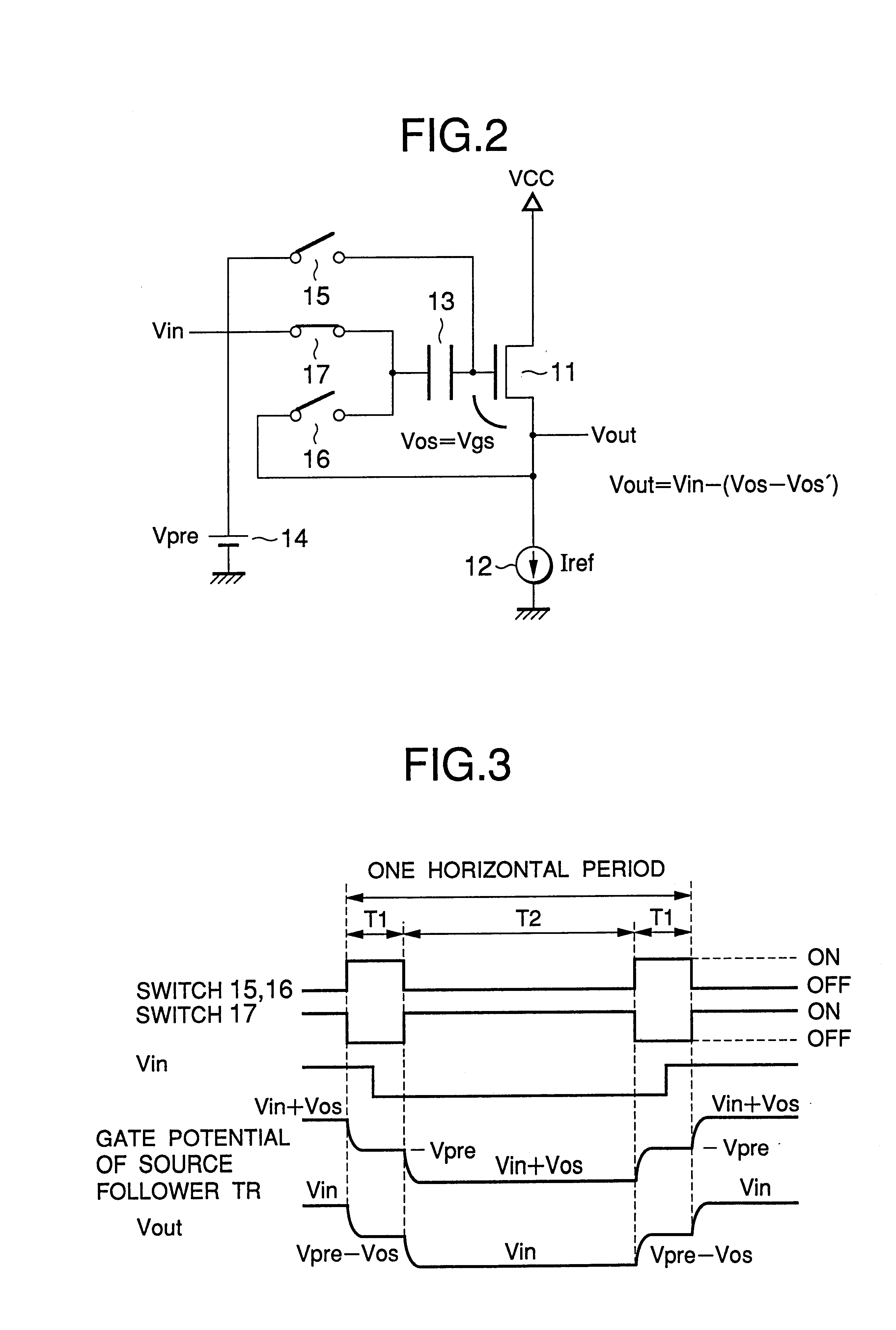
In the first embodiment in FIG. 2, a source follower circuit has an NMOS source follower transistor 11 connected to a power supply VCC with the drain thereof and a current source 12 connected across the source of the source follower transistor 11 and earth. The gate of the source follower transistor 11 is connected to one end of a capacitor 13. The first analog switch 15 is connected across the gate of the source follower transistor 11 and a precharge supply 14. The second analog switch 16 is connected across the other end of the capacitor 13 and the source of the source follower transistor 11. The third analog switch 17 is connected across the other end of the capacitor 13 and a signal source (Vin).

The first analog switch 15 and the second analog switch 16 are simultaneously operated, i.e. turned on (closed) and off (open) in the same periods. The third analog switch 17 is operated in reverse with respect to the opening and closing of the first and second analog switches 15 and 16....

second embodiment

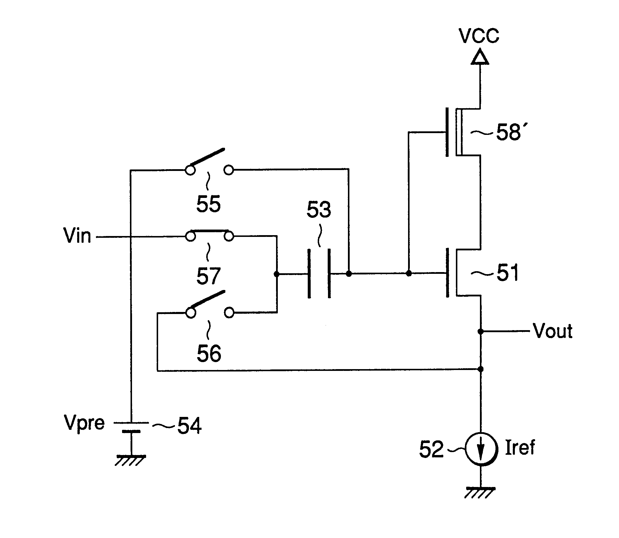
In this second embodiment, however, the gate-drain voltage Vgd of the source follower transistor 51 can be kept substantially fixed even in the precharge period as well as in the output period for outputting an arbitrary signal by cascode connecting the NMOS transistor 58 to the drain side of the source follower transistor 51 and connecting the PMOS source follower transistor 59 across the gate of the source follower transistor 51 and the gate of the cascode connected transistor 58.

This is because the drain voltage Vd of the source follower transistor 51 is a function of the gate voltage Vg, the gate-source voltage Vgs58 of the cascode connected transistor 58 and the gate-source voltage Vgs59 of the source follower transistor 59 which can be expressed as

and the drain voltage Vd of the source follower transistor 51 therefore changes in response to the change in the gate voltage Vg thereof.

Compared with the circuit configuration of the first embodiment, fluctuations in the drain volta...


PUM

PropertyMeasurementUnit
conduction typeaaaaaaaaaa
conductionaaaaaaaaaa
reference voltageaaaaaaaaaa

Abstract

In a source follower circuit having an NMOS source follower transistor with a drain thereof connected to a power supply and a current supply connected across the source of this transistor and earth, one end of a capacitor is connected to the gate of the transistor, the first analog switch is connected across the gate of the transistor and a precharge supply, the second analog switch is connected across the other end of the capacitor and the source of the transistor, and the third analog switch is connected across the other end of the capacitor and a signal source.

Description

BACKGROUND OF THE INVENTIONThe present invention relates to a liquid crystal display device, and more particularly relates to a source follower circuit constructed from a polysilicon thin film transistor (hereinafter referred to as a "polysilicon TFT" (Thin Film Transistor)) and an output circuit for the liquid crystal display device employing this source follower circuit as an output buffer.Output buffers for charging each column line capacitor in a liquid crystal display device are generally constructed with voltage follower circuits employing operational amplifiers. However, in integrally forming a liquid crystal panel and a driver circuit thereof using polysilicon, complicated circuits for the operational amplifiers and variation in characteristics and large threshold voltage Vth of polysilicon TFTs make it difficult to form voltage follower circuits with polysilicon. This causes difficulty in integrally forming a liquid crystal panel and a driver circuit thereof with polysilico...

Claims


Application Information

Patent Timeline
Patent Type & Authority Patents(United States)
IPC IPC(8): G09G3/36G02F1/133G09G3/20H03F3/50H03K19/0175
CPCG09G3/2011G09G3/3688G09G2310/0248G09G2310/027G09G2310/0291
Inventor MAEKAWA, TOSHIKAZUNAKAJIMA, YOSHIHARU
Owner SONY CORP
Why Eureka
Try Eureka