Semiconductor device and method for manufacturing the same
a technology of semiconductors and semiconductors, applied in the direction of instruments, optical waveguide light guides, optical light guides, etc., can solve the problems of difficult to obtain a good quality crystalline film, difficult to obtain the large amount of thickness variation with high accuracy, etc., and achieve the effect of large thickness variation and high accuracy
- Summary
- Abstract
- Description
- Claims
- Application Information
AI Technical Summary
Benefits of technology
Problems solved by technology
Method used
Image
Examples
first embodiment
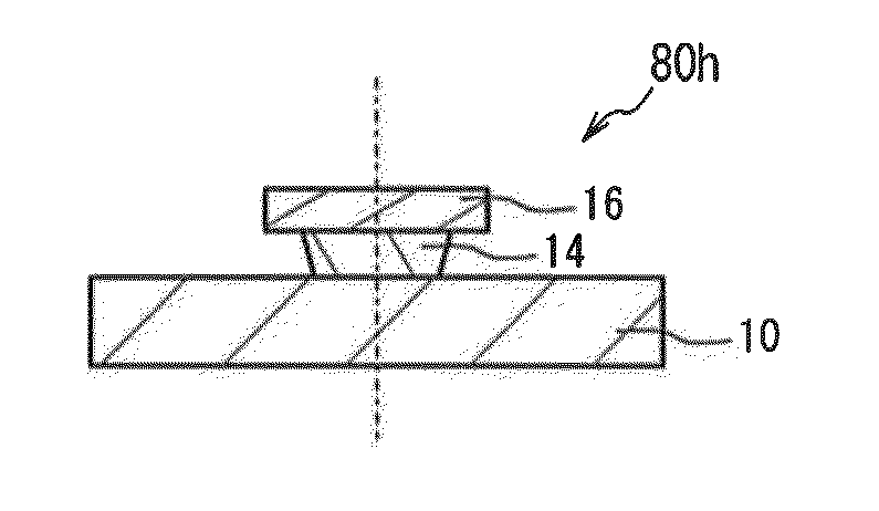
[0072]FIG. 5A is a plan view of a suspended mask 80 of the first embodiment in the present invention. FIG. 5B is a graph showing the relationship between the thickness T1 of the semiconductor layer formed using the suspended mask 80 and the position X. The thickness is taken along the line D-D of FIG. 5A. FIGS. 6A to 6C are a cross-sectional view taken along the line A-A of FIG. 5A, a cross-sectional view taken along the line BB of FIG. 5A, and a cross-sectional view taken along the line C-C of FIG. 5A, respectively, Referring to FIG. 5A, the suspended mask 80 is formed in a first region 50, a second region 52, a third region 54 and a fourth region 56. Referring to FIGS. 6A to 6C, the suspended mask 80 includes a first layer 14 and a second layer 16.
[0073]As shown in FIG. 5A, the first region 50 extends in the X direction, and the width W1 in the Y direction is changed along the X direction. The X direction corresponds to the first direction, and the Y direction corresponds to the s...
second embodiment
[0108]A semiconductor layer formed in the first embodiment is used in a waveguide for a spot-size converter. FIG. 16 is a block diagram of a system in which a semiconductor device 100 according to a second embodiment is used. As shown in FIG. 16, spot-size converters 91 and 92, a Mach-Zehnder modulator 93, waveguides 94 and 95, and an interconnection 102 are disposed on a substrate 90. The spot-size converters 91 and 92, the Mach-Zehnder modulator 93, the waveguides 94 and 95 and the substrate 10 are composed of semiconductors. The interconnection 102 is composed of a metal. A laser light 98 is radiated from a lensed fiber 96 onto the spot-size converter 91. The spot-size converter 91 converts the spot site of the laser light 98 into the size of the waveguide 95. The Mach-Zehnder modulator 93 modulates an optical signal propagated through the waveguide 94 using an electrical signal 103 propagated through the interconnection 102. The Mach-Zehnder 93 outputs a modulated light to the w...
third embodiment
[0130]FIGS. 33A to 33C shows the shape of a suspended mask 80g of the third embodiment. FIGS. 33A to 33C are cross-sectional views showing the process of forming a semiconductor layer in accordance with a third embodiment. FIGS. 33A to 33C show a first region 50 and fourth regions 56. In the third embodiment, a second layer 16a is made of an insulating layer. As the second layer 16a, for example, a silicon dioxide film or a silicon nitride film is used. In FIGS. 33A to 33C, the solid line in the semiconductor layer 12 indicates the surface of the semiconductor layer 12 formed using the suspended mask 80g. The broken line indicate the semiconductor layer 12 of the first embodiment in which the second layer 16 is composed of a semiconductor.
[0131]When the second layer 16a is formed of an insulating layer, no semiconductor layer is formed around the second layer 16a. On the other hand, as shown in FIGS. 6A to 6C in the first embodiment, the semiconductor layer 86 is formed on and under...
PUM
 Abstract
Description
Claims
Application Information


