Method for obtaining a thin film in particular semiconductor, comprising a protected ion zone and involving an ion implantation

a technology of ion implantation and semiconductor, applied in the direction of transistors, electrical devices, solid-state devices, etc., can solve problems such as defects that modify the characteristics of components

Inactive Publication Date: 2001-11-13
COMMISSARIAT A LENERGIE ATOMIQUE ET AUX ENERGIES ALTERNATIVES
View PDF16 Cites 85 Cited by
  • Summary
  • Abstract
  • Description
  • Claims
  • Application Information

AI Technical Summary

Problems solved by technology

However, the implantation of ions through electrically active layers may create defects that modify the characteristics of the components, or make them unusable.

Method used


Image

  • Method for obtaining a thin film in particular semiconductor, comprising a protected ion zone and involving an ion implantation
  • Method for obtaining a thin film in particular semiconductor, comprising a protected ion zone and involving an ion implantation
  • Method for obtaining a thin film in particular semiconductor, comprising a protected ion zone and involving an ion implantation

Examples


Embodiment Construction

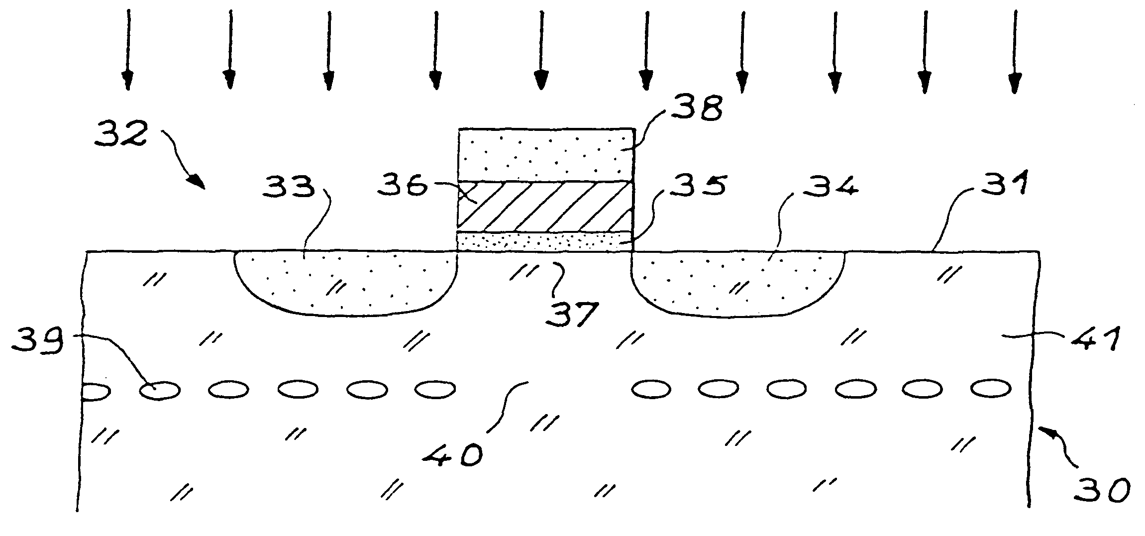
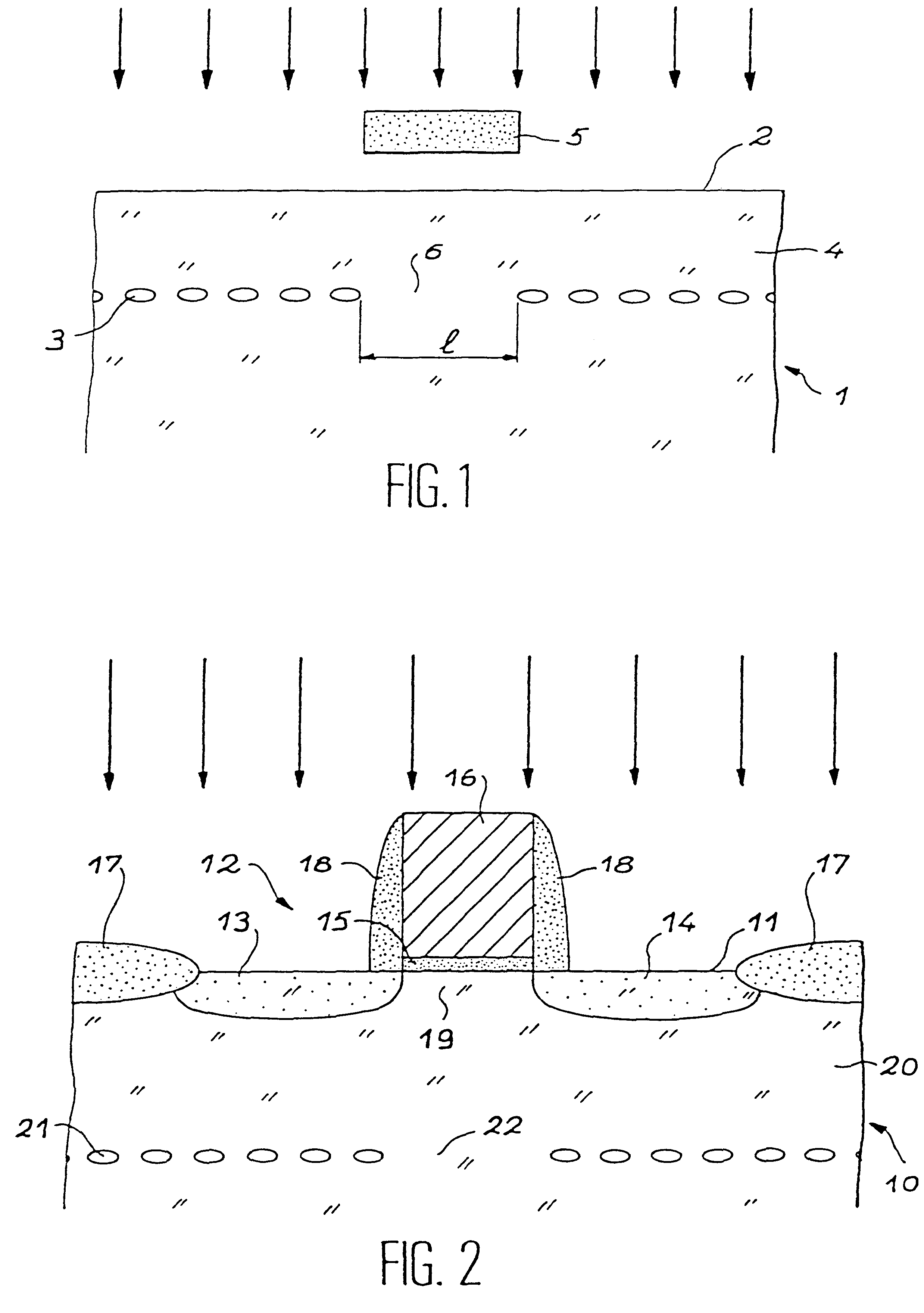
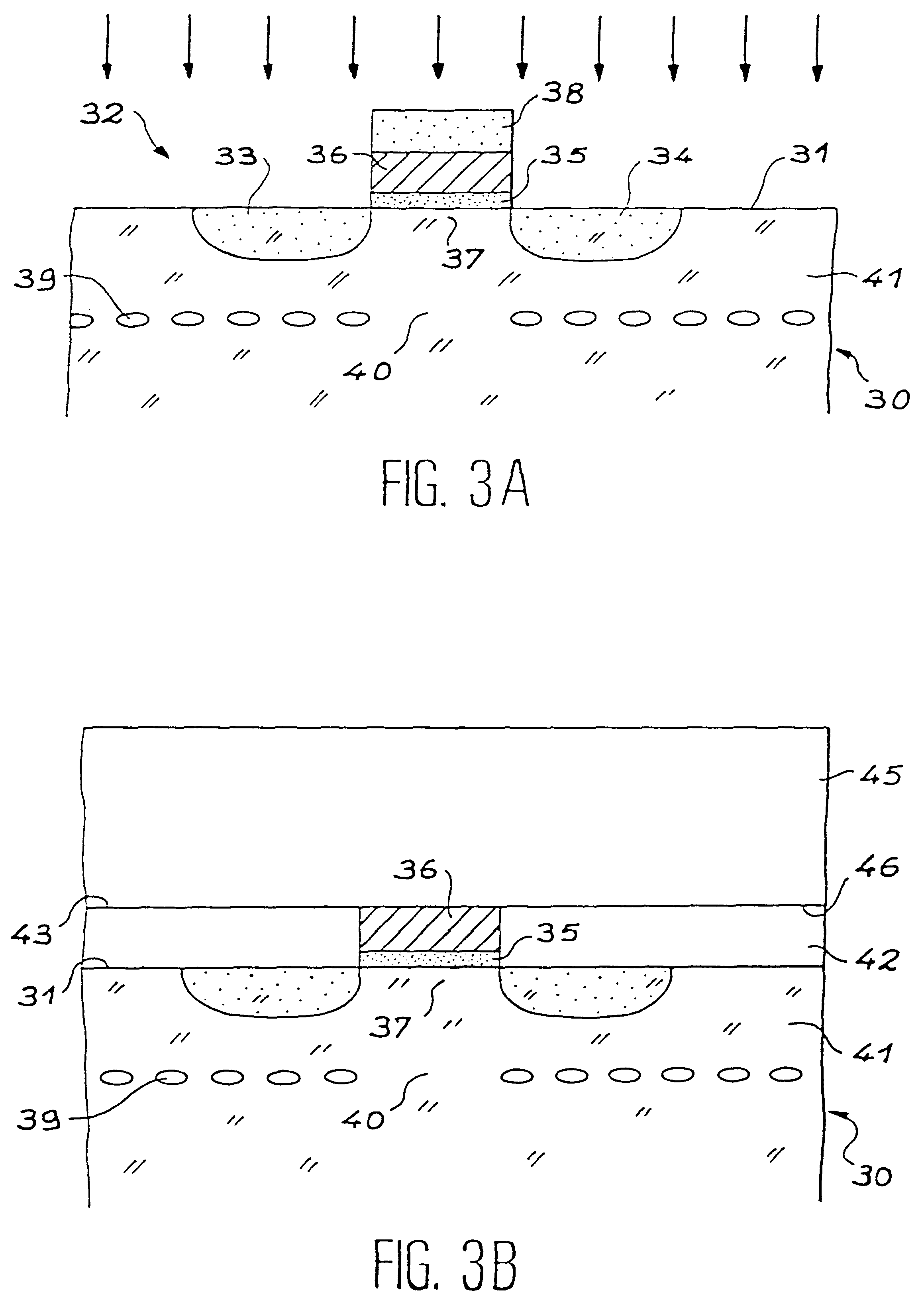
Thus, the process divulged by document FR-A-2 681 472, which is technically very interesting, had limitations in some of these applications. The inventors of this patent have found a solution to this problem. They have discovered that under some conditions, a masking technique can be used to protect areas sensitive to the transfer of ions, which implies an absence of micro-cavities in the areas corresponding to the masked areas, and nevertheless obtaining cleavage in the substrate so that a thin film can be detached, This is possible if the width of each masked area does not exceed a limiting dimension determined for the material making up the substrate. This principle can also be applied to structures in which elements have been made before implantation, these elements masking areas of the substrate that are not necessarily sensitive to the implantation. In this case, the purpose of the invention is to make these elements significantly narrower than or equal to the limiting dimensi...


PUM


Abstract

The invention relates to a process for obtaining a thin film from a substrate, the film being delimited in the substrate by ionic implantation and by heat treatment inducing a fracture line along which the film can be separated from the rest of the substrate. A particular area, for example composed of a gate oxide layer (15) and the channel area (19) of a MOS transistor (12) created in the substrate region (10) intended to form the tin film (20), this area may be protected by ionic implantation by masking using the transistor gate (16), which does not prevent the fracture from occurring provided that the width of the area does not exceed a limiting dimension determined for the material forming the substrate.

Description

TECHNICAL DOMAINThis invention relates to a process for obtaining a thin film, comprising an area protected from ions, involving an ionic implantation step. In particular it relates to obtaining a semiconducting thin film in which active layers are created, for example to create MOS transistor channel areas.STATE OF PRIOR ARTIn the subject of semiconductors, it is sometimes necessary to make semiconducting thin films, for example to make "Silicon On Insulator" substrates. Other methods of making thin semiconducting films have been developed. One of the most recent methods is based on the fact that implantation of ions of a rare gas or hydrogen in a semiconducting material induces the formation of brittle zones at a depth close to the average ion penetration depth. Document FR-A-2 681 472 divulges a process that uses this property to obtain a thin film of semiconducting material. This process consists of applying the following steps to a platelet of the required semiconducting materi...

Claims


Application Information

Patent Timeline
Patent Type & Authority Patents(United States)
IPC IPC(8): H01L29/66H01L21/02H01L21/336H01L29/786H01L21/265H01L27/12
CPCH01L29/66772H01L29/78654H01L21/2007H01L21/18
Inventor BRUEL, MICHELASPAR, BERNARD
Owner COMMISSARIAT A LENERGIE ATOMIQUE ET AUX ENERGIES ALTERNATIVES
Why Eureka
Try Eureka