Method for manufacturing a chip scale package having copper traces selectively plated with gold

a scale package and scale technology, applied in the direction of semiconductor devices, semiconductor/solid-state device details, electrical equipment, etc., can solve the problems of not being reliable in bga packages as some conventional packages, and occupying space on the board for mounting semiconductor chips

Inactive Publication Date: 2001-11-20
SAMSUNG ELECTRONICS CO LTD
View PDF3 Cites 18 Cited by
  • Summary
  • Abstract
  • Description
  • Claims
  • Application Information

AI Technical Summary

Benefits of technology

In accordance with a first embodiment of the present invention, a method for manufacturing a chip scale package includes: (A) preparing a tape wiring board that comprises a strip of polyimide tape having top and bottom surfaces, Cu traces formed on the bottom surface of the polyimide tape, a window formed in the polyimide tape to enable Cu traces extending across the window to be connected to a semiconductor chip through the window, multiple connection holes formed in the polyimide tape to expose portions the of Cu traces for solder ball attachment, and an elastomer chip carrier attached to the bottom surface of the tape inside of the window; (B) applying a "pre-flux" solution to the portions of the Cu traces exposed through the connection holes to prevent them from being plated with Au; (C) defining beam leads by Au-plating portions of the Cu traces extending across the window; (D) attaching a semiconductor chip to the bottom surface of the elastomer chip carrier such that a peripheral portion of the chip overhangs the carrier and is exposed below the window; (E) bonding the beam leads to the semiconductor chip through the window; (F) encapsulating the bonding area between the beam leads and the semiconductor chip; and, (G) attaching solder balls to the respective portions of the Cu traces exposed through the connection holes.

Problems solved by technology

In some respects, however, the BGA package is not as reliable as some conventional packages.
Another disadvantage of the BGA package is that space must be reserved on the board for mounting the semiconductor chip.

Method used


Image

  • Method for manufacturing a chip scale package having copper traces selectively plated with gold
  • Method for manufacturing a chip scale package having copper traces selectively plated with gold
  • Method for manufacturing a chip scale package having copper traces selectively plated with gold

Examples


first embodiment

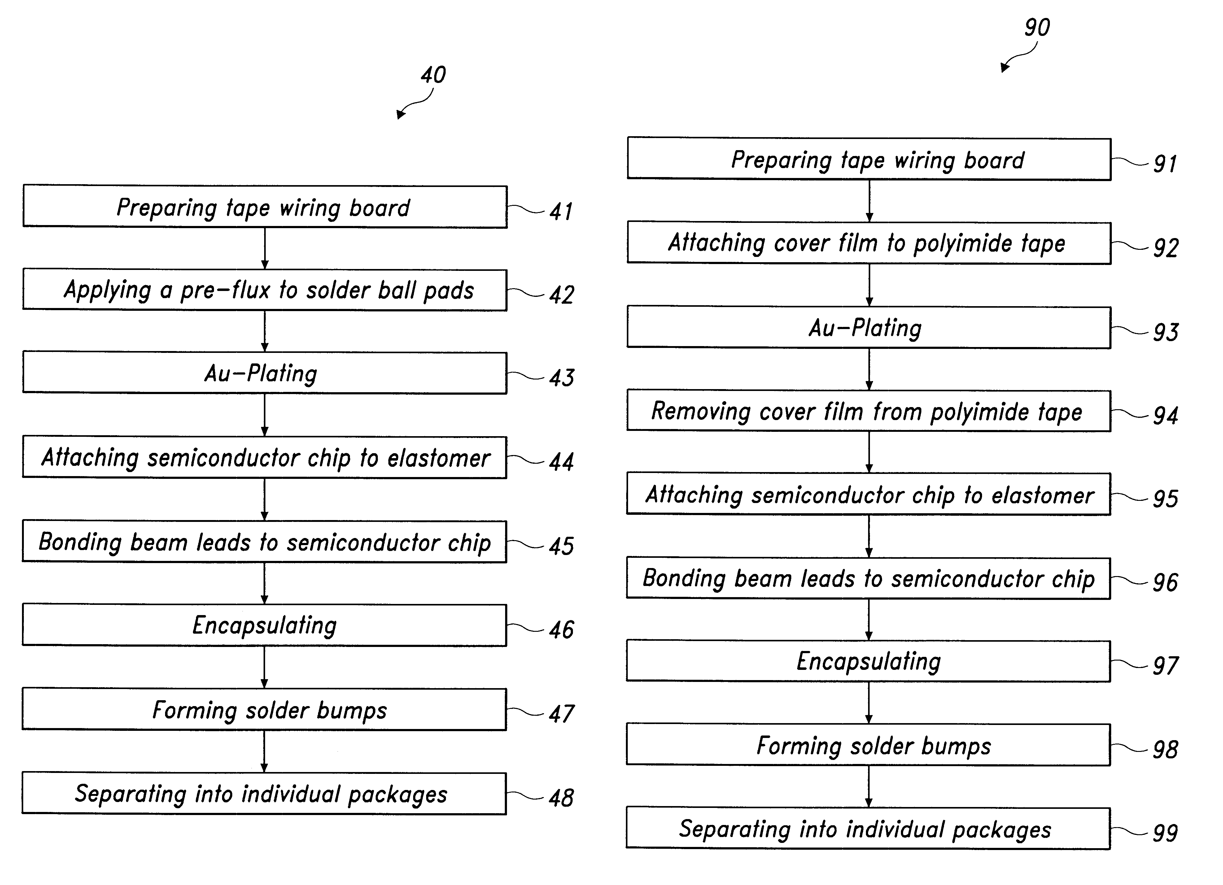
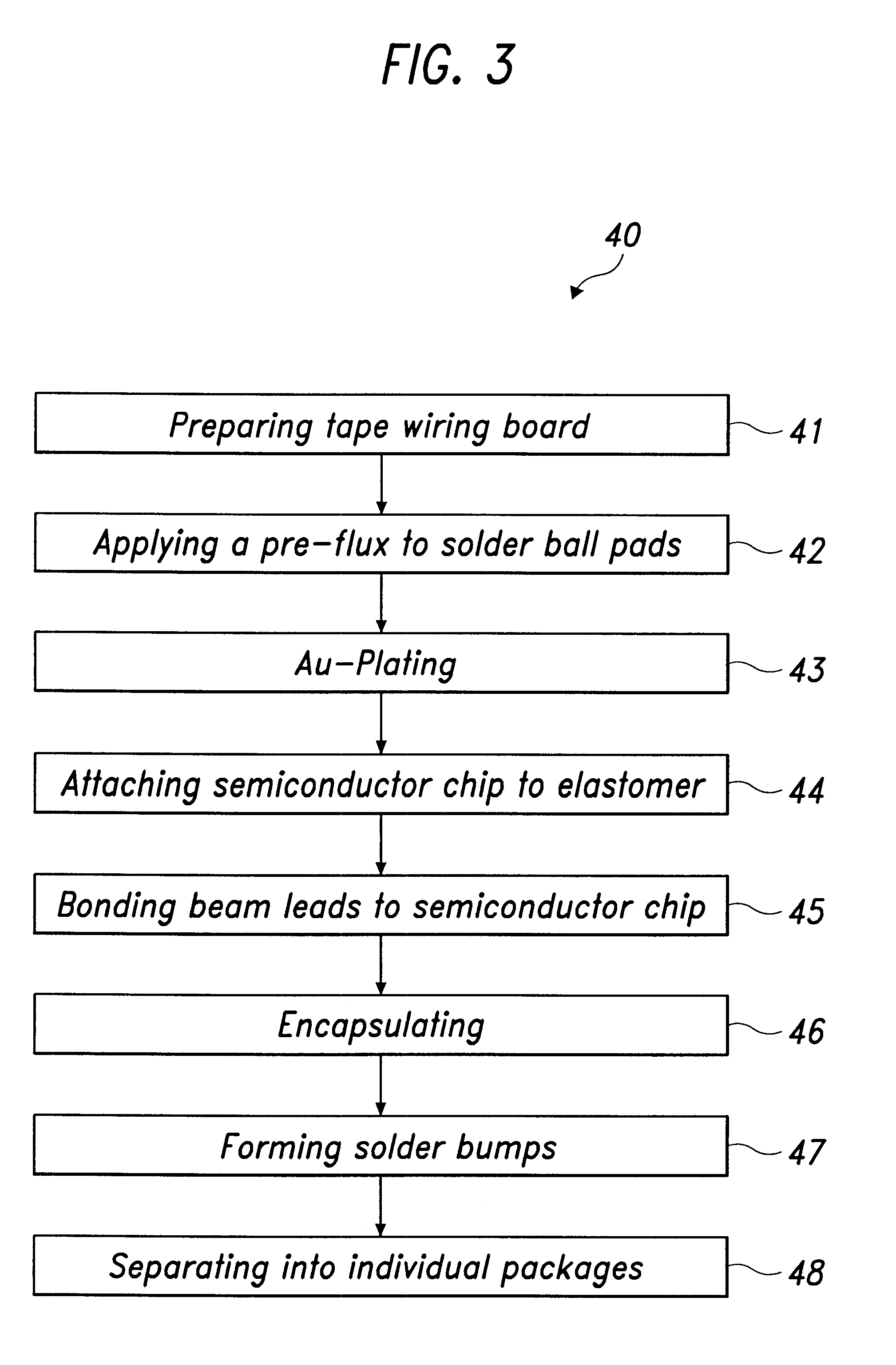
With reference to FIGS. 3 to 12, a method 40 for manufacturing a chip scale package according to the present invention comprises the following:

As shown schematically in FIG. 3, the first method 40 starts with preparing a tape wiring board 20 having an elastomer chip carrier 50 attached to its bottom surface (step 41). As shown in FIGS. 4 and 5, the wiring board 20 is manufactured by attaching a thin copper film to the bottom surface of a strip of polyimide tape 24 with an adhesive 21 and patterning the copper film by using a photolithography method. The wiring board 20 includes a polyimide tape 24, and Cu traces 30 that are formed by the photolithography of the copper film. Typically, the wiring board strip includes a plurality of identical wiring boards 20 connected to each other in a matrix, or "ganged," form for economy of manufacture.

The polyimide tape 24 includes an inner portion 24a that has a plurality of connection holes 23 formed through the thickness of the tape, a window ...

second embodiment

FIG. 13 is a flowchart of another method 90 for manufacturing a chip scale package according to the present invention. The second method 90 differs from the first method 40 of FIG. 3 in that the second method 90 employs a temporary cover film over the solder ball pads instead of the pre-flux to prevent the solder ball pads from being plating with Au. Thus, step 91 in FIG. 13 of the second method, preparing the wiring board, is identical to step 41 in FIG. 3 of the first method.

Referring to FIGS. 14 and 15, after preparing the tape wiring board 20, a cover film 84 is attached to the top surface of the inner part 24a to prevent the Au-plating of the solder ball pads 36 (FIG. 13, step 92). Beam leads 60 are defined by plating the outer wiring patterns 38 in the window 22 with Au to about 1 .mu.m thickness (step 93). The cover film 84 is removed after Au plating (step 94). To facilitate film removal, the cover film can be provided with a special adhesive layer. For example, an adhesive ...


PUM


Abstract

A method for manufacturing a chip scale package comprises preparing a tape wiring board that includes a polyimide tape having top and bottom surfaces, Cu traces formed on the bottom surface of the tape, a window formed in the tape to enable the Cu traces to be connected to a semiconductor chip attached below the board, multiple connection holes formed in the tape to expose portions of the Cu traces therethrough and define solder ball mounting pads, and an elastomer chip carrier attached to the bottom surface of the tape. The method includes applying either a pre-flux or a cover sheet over the solder ball mounting pads. The pre-flux and the cover sheet each prevents the solder ball mounting pads being plated with gold. This, in turn, prevents the formation of intermetallic compounds in the solder balls so that the bond strength between the solder balls and a pad to which they attach is improved.

Description

BACKGROUND1. Field of the InventionThe present invention generally relates to a method for manufacturing semiconductor packages, and more particularly, for manufacturing a chip scale package ("CSP").2. Description of the Related ArtElectronic industry trends, such as miniaturization and multifunctionalization of electronic devices, have resulted in a relatively new semiconductor package called a Ball Grid Array ("BGA") package. When compared to conventional plastic packages, the BGA package has a higher surface-mounting density and superior electrical capabilities. In some respects, however, the BGA package is not as reliable as some conventional packages. Unlike a conventional plastic package that uses moisture-resistant lead frames, the BGA package uses a printed circuit board that is more moisture-prone. Another disadvantage of the BGA package is that space must be reserved on the board for mounting the semiconductor chip. In view of the foregoing drawbacks, a Chip Scale Package ...

Claims


Application Information

Patent Timeline
Patent Type & Authority Patents(United States)
IPC IPC(8): H01L23/28H01L23/31H01L23/495H01L23/48H01L21/60H01L23/12
CPCH01L23/3114H01L23/49572H01L23/49582H01L24/50H01L2224/131H01L2224/13144H01L2924/01004H01L2924/01006H01L2924/01029H01L2924/0105H01L2924/01075H01L2924/01078H01L2924/01079H01L2924/01082H01L2924/01327H01L2924/12044H01L2924/15311H01L2924/014H01L2924/00014H01L2924/01005H01L2924/01033H01L2924/12042H01L24/86H01L2924/00H01L21/60
Inventor JEONG, DO SOOSOHN, HAI JEONGLEE, DONG HO
Owner SAMSUNG ELECTRONICS CO LTD
Why Eureka
Try Eureka