Pattern Transfer Printing by Kinetic Control of Adhesion to an Elastomeric Stamp

Active Publication Date: 2009-08-13
THE BOARD OF TRUSTEES OF THE UNIV OF ILLINOIS
View PDF27 Cites 281 Cited by
  • Summary
  • Abstract
  • Description
  • Claims
  • Application Information

AI Technical Summary

Benefits of technology

[0007]The present invention provides methods, systems and system components for transferring, assembling and integrating features and arrays of features having selected nanosized and/or microsized physical dimensions, shapes and spatial orientations. Methods of the present invention utilize principles of ‘soft adhesion’ to guide the transfer, assembly and/or integration of features, such as printable semiconductor elements or other components of electronic devices. Methods of the present inventi

Problems solved by technology

The most significant challenges associated with realizing these types of system derive from the disparat

Method used


Image

  • Pattern Transfer Printing by Kinetic Control of Adhesion to an Elastomeric Stamp
  • Pattern Transfer Printing by Kinetic Control of Adhesion to an Elastomeric Stamp
  • Pattern Transfer Printing by Kinetic Control of Adhesion to an Elastomeric Stamp

Examples


example 1

Transfer Printing onto Semiconductor Wafers

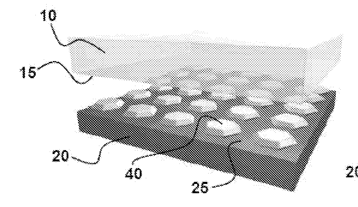
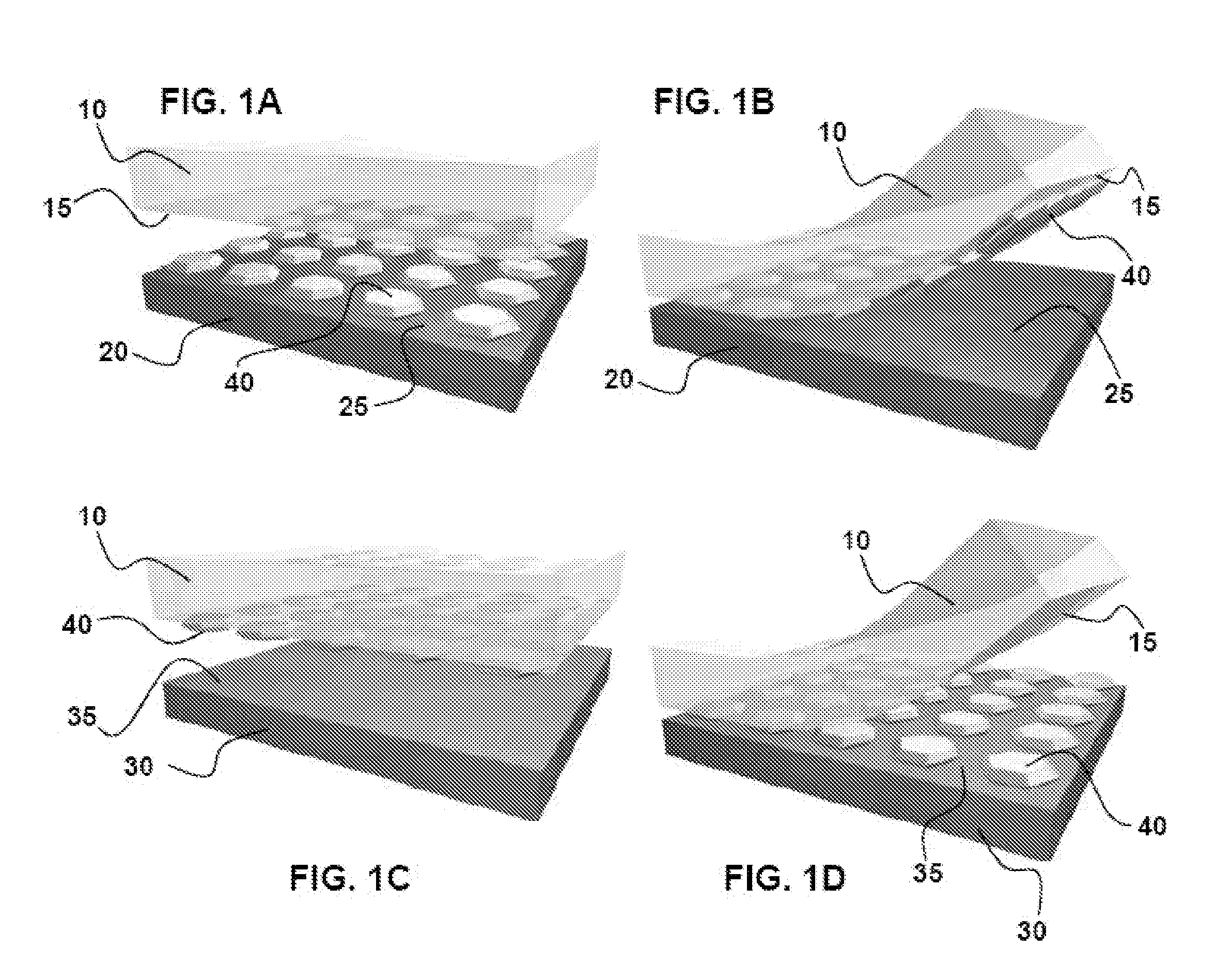
[0113]The present invention encompasses methods that transfer prints a plurality of structures from a donor substrate surface to a receiving substrate surface. For example, FIG. 4 shows a 30 mm×38 mm GaAs wafer printed with an array of I-shaped silicon microstructures (see inset) by a single elastomeric stamp. In a single step, an inked elastomeric stamp prints the pattern in ambient conditions directly onto a 100-mm GaAs wafer. This array contains about 24,000 microstructures; the yield of the entire process, including micromachining, pick-up and printing, is more than 99.5% (corresponding to fewer than 100 microstructures missing from the array). Particles on the surface of the receiving substrate are typically the most significant cause of defects. With care, including careful processing and handling of the receiving substrate, printing efficiency can approach 100%.

[0114]Unlike wafer-bonding approaches to semiconductor materials integrat...

example 2

Transfer Printing of Sheet-Like Geometries

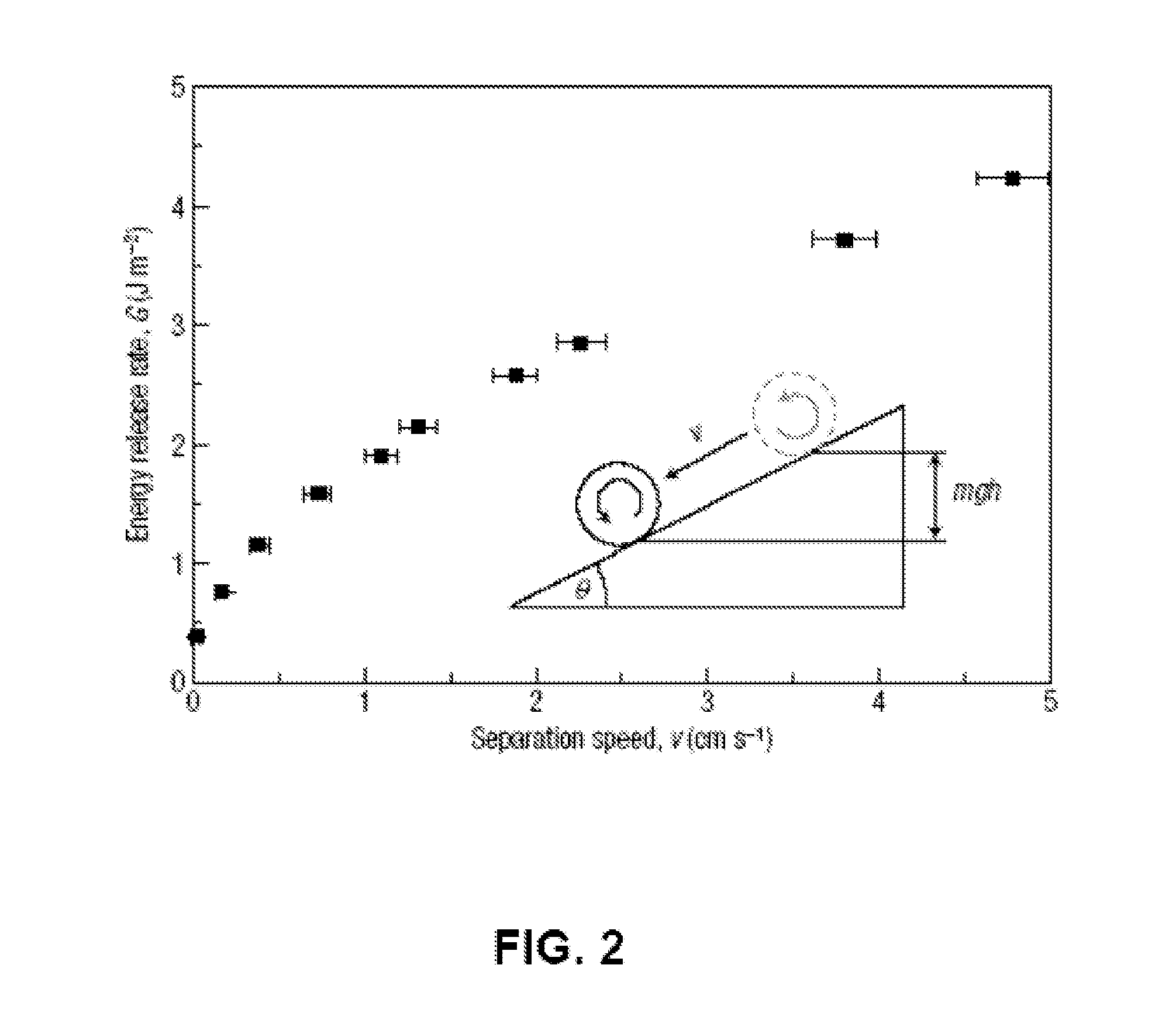
[0118]The strong adhesion of features to the stamp at high separation rates is essential to achieve reliable, high-yield printing of the classes of objects illustrated in Example 1. This adhesion can be sufficiently strong, in fact, to remove material structures that are ionically bonded to the donor substrate along their entire lengths. FIG. 11 shows, as an example, a pattern of thin high-quality muscovite (grade V-1 mica) printed by removing a stamp in contact with the mica at sufficiently high separation rates to cleave patterned ribbons from a donor substrate of bulk mica. PDMS stamps can also cleave sheets from unpatterned grade V-1 mica or graphite (FIG. 12) and lift off mica sheets bonded to SiO2, indicating that the stamp-microstructure interface is strong enough at high separation rates to remove structures bound to a donor substrate at least as strongly as 6 J / m2. The high adhesive strength present at high separation rates reduces ...

example 3

Transfer Printing of Globular Geometries

[0119]The transfer devices disclosed herein can pick-up and release, for example, highly non-planar, globular structures, such as silica microspheres (FIG. 13) and grains of pollen (FIG. 14), which have very small areas of contact to rigid receiving substrates.


PUM

PropertyMeasurementUnit
Lengthaaaaaaaaaa
Lengthaaaaaaaaaa
Lengthaaaaaaaaaa

Abstract

The present invention provides methods, systems and system components for transferring, assembling and integrating features and arrays of features having selected nanosized and/or microsized physical dimensions, shapes and spatial orientations. Methods of the present invention utilize principles of ‘soft adhesion’ to guide the transfer, assembly and/or integration of features, such as printable semiconductor elements or other components of electronic devices. Methods of the present invention are useful for transferring features from a donor substrate to the transfer surface of an elastomeric transfer device and, optionally, from the transfer surface of an elastomeric transfer device to the receiving surface of a receiving substrate. The present methods and systems provide highly efficient, registered transfer of features and arrays of features, such as printable semiconductor element, in a concerted manner that maintains the relative spatial orientations of transferred features.

Description

CROSS-REFERENCE TO RELATED APPLICATIONS[0001]This application is a continuation-in-part of U.S. patent application Ser. Nos. 11 / 145,542, filed Jun. 2, 2005 and U.S. patent application Ser. No. 11 / 145,574, filed Jun. 2, 2005, both of which claim the benefit under 35 U.S.C. 119(e) of U.S. Provisional Patent Application Nos. 60 / 577,077, 60 / 601,061, 60 / 650,305, 60 / 663,391 and 60 / 677,617 filed on Jun. 4, 2004, Aug. 11, 2004, Feb. 4, 2005, Mar. 18, 2005, and May 4, 2005, respectively, all of which are hereby incorporated by reference in their entireties to the extent not inconsistent with the disclosure herein.STATEMENT REGARDING FEDERALLY SPONSORED RESEARCH OR DEVELOPMENT[0002]This invention was made, at least in part, with United States governmental support awarded by National Science Foundation under grant DMI-0328162, DARPA-funded AFRL-managed Macroelectronics Program Contract FA8650-04-C-7101, the US Department of Energy under grant DEFG02-91-ER45439. The United States government has...

Claims


Application Information

Patent Timeline
IPC IPC(8): H01L21/02
CPCB82Y10/00B82Y20/00H01L2924/13091H01L29/0665H01L29/0673H01L29/1606H01L29/78603H01L31/035281H01L31/0392H01L31/072H01L31/109H01L31/18H01L31/1804H01L31/1892H01L2924/12041Y02E10/547H01L2924/00H01L31/03925Y02P70/50
Inventor NUZZO, RALPH G.ROGERS, JOHN A.MENARD, ETIENNELEE, KEON JAEKHANG, DAHL-YOUNGSUN, YUGANGMEITL, MATTHEWZHU, ZHENGTAO
Owner THE BOARD OF TRUSTEES OF THE UNIV OF ILLINOIS
Why Eureka
Try Eureka