Method for making a thin film on a support and resulting structure including an additional thinning stage before heat treatment causes micro-cavities to separate substrate element
- Summary
- Abstract
- Description
- Claims
- Application Information
AI Technical Summary
Benefits of technology
Problems solved by technology
Method used
Image
Examples
Embodiment Construction
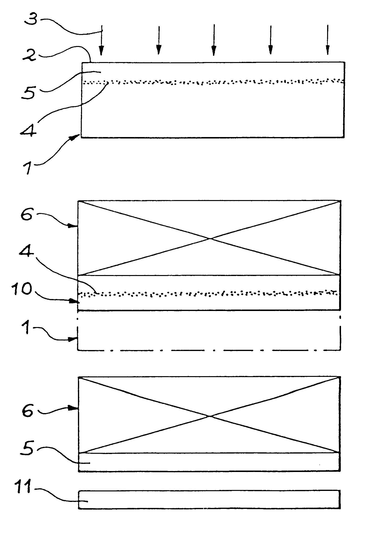
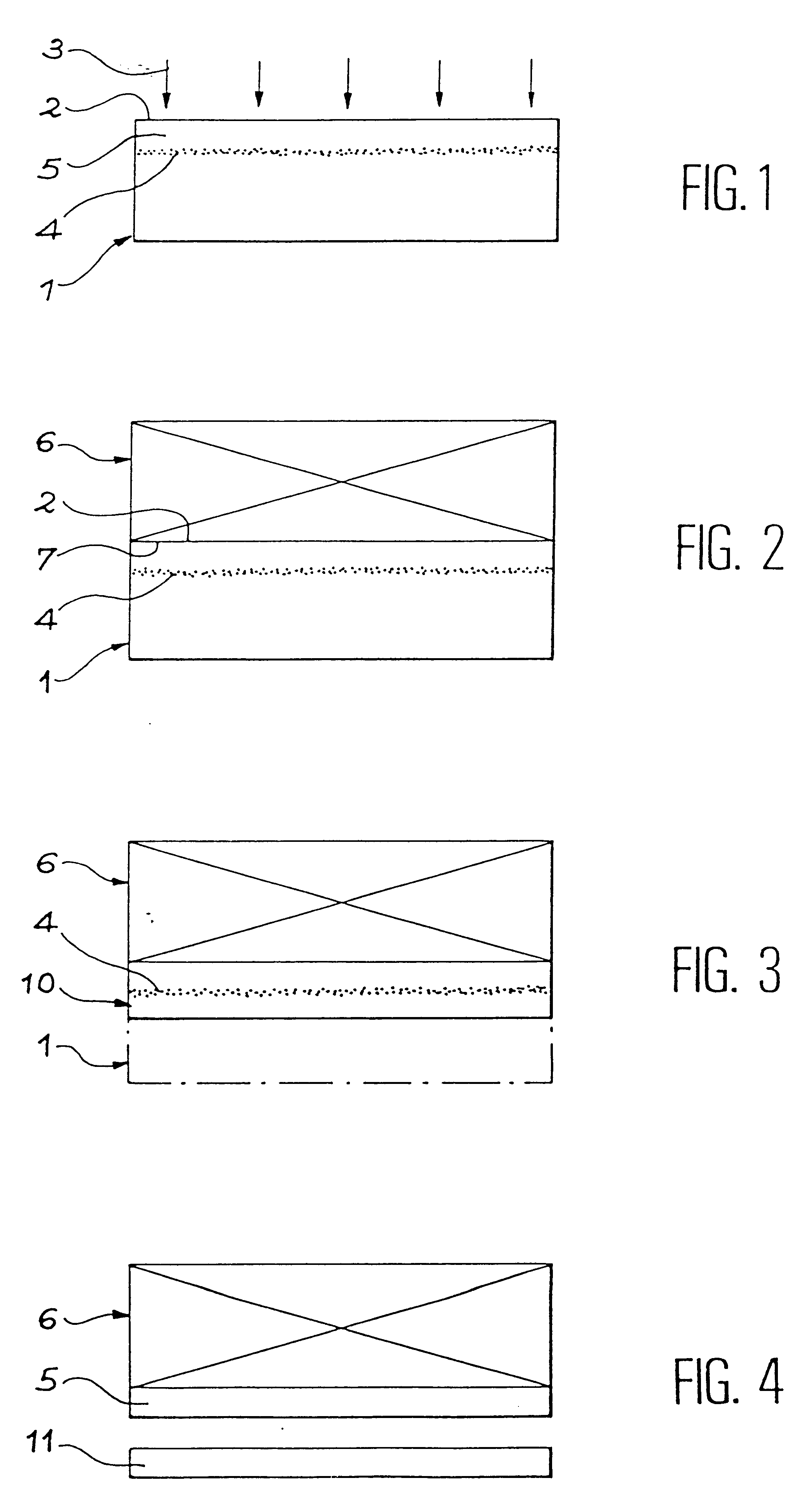
In the following section of the description, and as an example, the thinning stage is applied to the substrate in which the thin film is shaped by ionic implantation. Said thinning must be a compromise between minimum thinning of the substrate, that is required in order to avoid the thin film separating from the support in the heat treatment stage, and maximum thinning beyond which there is a risk, during the heat treatment, of the micro-bubbles (micro-cavities) moving towards the face of the thinned substrate and consequently causing blisters.
The substrate is not necessarily a semiconductor substrate. When the substrate is a semiconductor it can comprise elements of integrated circuits.
The application of the method disclosed in French document 2 681 472 for silicon coating, for example monocrystalline, onto a support (or stiffener) can be achieved by completely different means according to the nature of the material that constitutes the support. If the support must be made of glass...
PUM
 Abstract
Description
Claims
Application Information
 - R&D
- Intellectual Property
- Life Sciences
- Materials
- Tech Scout
- Unparalleled Data Quality
- Higher Quality Content
- 60% Fewer Hallucinations
Browse by: Latest US Patents, China's latest patents, Technical Efficacy Thesaurus, Application Domain, Technology Topic, Popular Technical Reports.
© 2025 PatSnap. All rights reserved.Legal|Privacy policy|Modern Slavery Act Transparency Statement|Sitemap|About US| Contact US: help@patsnap.com


