Semiconductor device and method of fabrication thereof, circuit board, and electronic equipment

a technology of semiconductor devices and semiconductor devices, applied in semiconductor devices, semiconductor/solid-state device details, electrical equipment, etc., can solve the problems of insufficient contact area of the bump formed by tearing off the wire, inability to ensure that the bump has a sufficiently flat upper surface, and inability to ensure the connection accuracy

Inactive Publication Date: 2002-01-01
SEIKO EPSON CORP
View PDF8 Cites 115 Cited by
  • Summary
  • Abstract
  • Description
  • Claims
  • Application Information

AI Technical Summary

Problems solved by technology

However, it is not possible to guarantee that a bump formed by tearing off a wire has a sufficiently flat upper surface.
This causes no problems when semiconductor chip are bonded face-down to a substrate, but it does cause problems in that connection accuracy de

Method used


Image

  • Semiconductor device and method of fabrication thereof, circuit board, and electronic equipment
  • Semiconductor device and method of fabrication thereof, circuit board, and electronic equipment
  • Semiconductor device and method of fabrication thereof, circuit board, and electronic equipment

Examples


first embodiment

FIGS. 1A to 6 are views for illustrating a first embodiment to which this invention is applied. In this method of fabricating a semiconductor device in accordance with this embodiment, the TAB technique is used. In addition, the semiconductor device to which a T-BGA package is applied is fabricated.

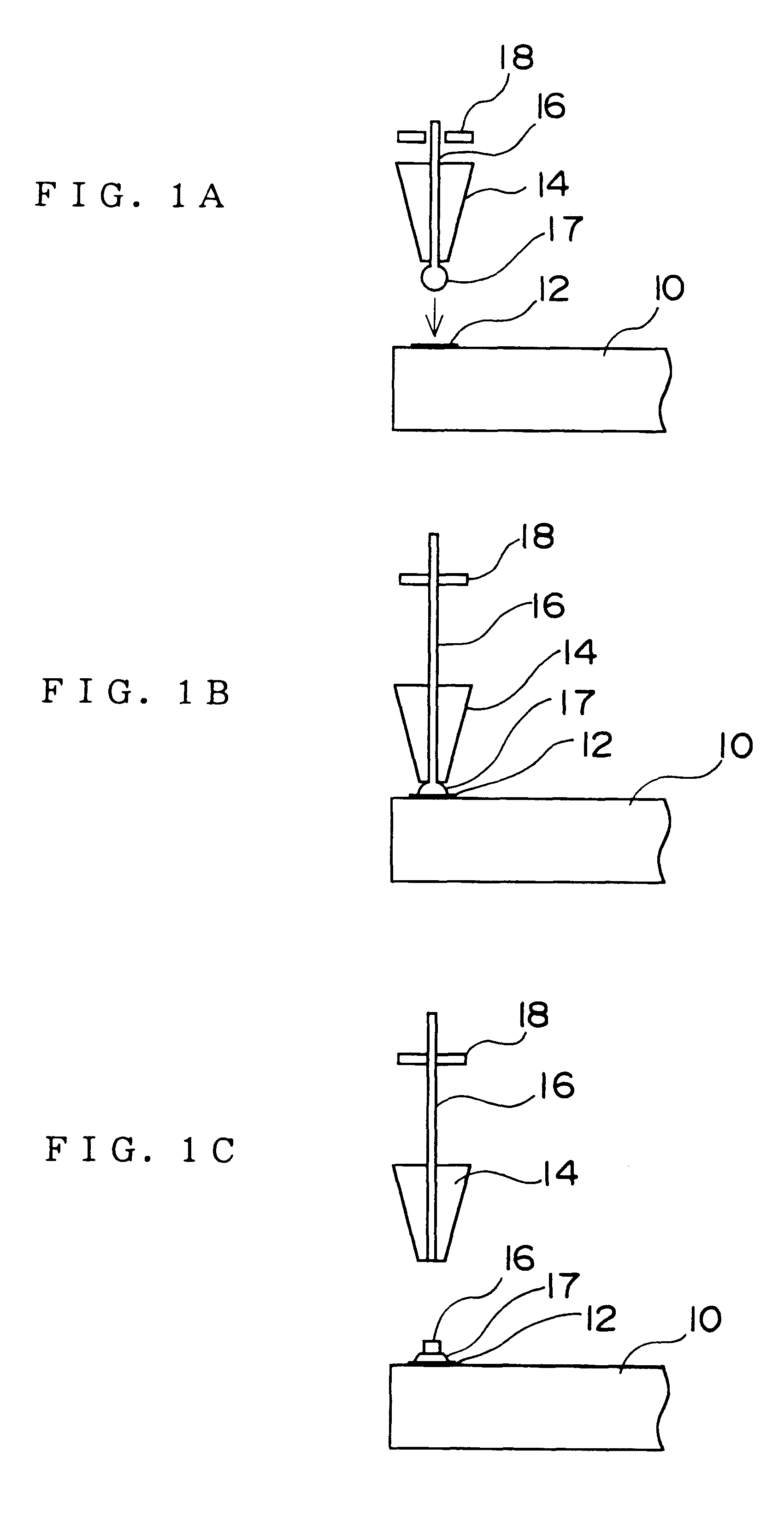
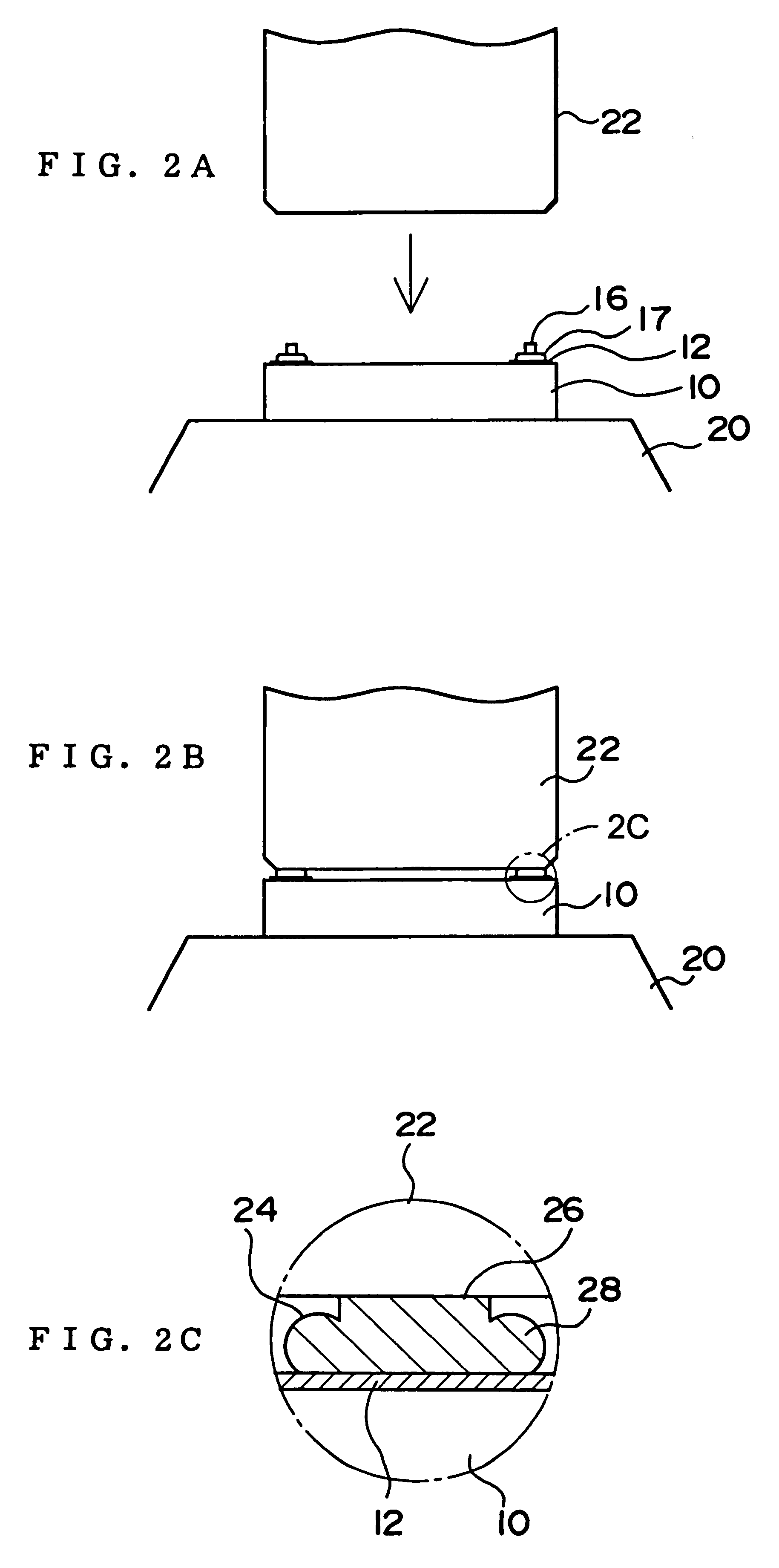
A step of forming a bump on an electrode of the semiconductor chip is shown in FIGS. 1A to 2B. First of all, a semiconductor chip 10 is provided, on which is formed one or a plurality of electrodes 12, as shown in FIG. 1A. Each electrode 12 is normally formed of a material such as aluminum, in a flat and thin shape on a surface of the semiconductor chip 10 on which active elements are formed. The shape of the side surfaces or cross-sectional surfaces thereof are not specifically limited if the electrode does not have a shape of a bump. The top surface of the electrode may be at the same height as the top surface of the semiconductor chip 10. The shape of a flat surface of the electrode 12...

second embodiment

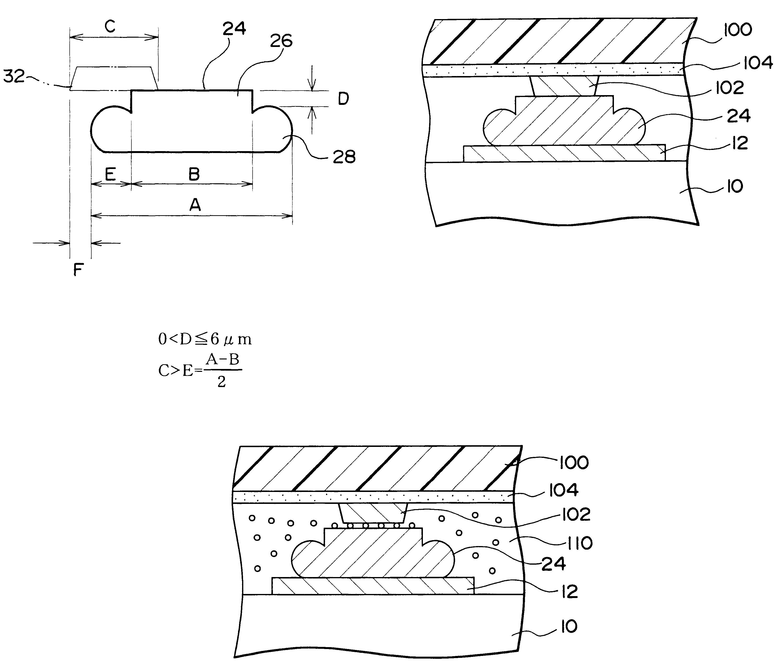
A semiconductor device in accordance with a second embodiment of this invention is shown in FIG. 7. The semiconductor chip 10 on which are formed the electrodes 12 is also used in this embodiment, and the bumps 24 are formed on the electrodes 12. The structure and method of formation of these bumps 24 are as already described with reference to the first embodiment.

A lead 102 is formed on a substrate 100. The material of the substrate 100 can be selected from those materials that can be used for the substrate 30 of the first embodiment. A three-layer substrate wherein the lead 102 is affixed by an adhesive 104 could also be used as the substrate 100. Alternatively, the lead could be formed by sputtering an electrically conductive film of copper or the like onto a substrate, then etching it. In such a case, the lead is formed directly on the substrate to form a two-layer substrate with no adhesive therebetween. Further alternatively, an additive process could be used to form the lead ...

third embodiment

A semiconductor device in accordance with a third embodiment of this invention is shown in FIG. 8. The semiconductor chip 10 on which are formed the electrodes 12 is also used in this embodiment, and the bumps 24 are formed on the electrodes 12. The structure and method of formation of these bumps 24 are as already described with reference to the first embodiment. The substrate 100 and the lead 102 are as already described with reference to the second embodiment.

The semiconductor chip 10 is bonded by either face-down bonding or flip-chip bonding onto the substrate 100, with an anisotropic conductive material 110 therebetween. The anisotropic conductive material 110 comprises conductive particles (electrically conductive filler) dispersed in an adhesive (binder), so a dispersive agent could also be added thereto. The anisotropic conductive material 110 could be formed beforehand as a sheet that is affixed to at least one of the substrate 100 and the semiconductor chip 10, or it could...


PUM


Abstract

A method of fabricating a semiconductor device including: a first step of bonding a conductive wire to any one of a plurality of electrodes of a semiconductor chip; a second step of tearing off the bonded conductive wire in such a manner that a part remains on one of the electrodes; a third step of pressing the part of the conductive wire remaining on the one of the electrodes, to form a bump having a head portion and a base portion; and, a fourth step of bonding a lead to the bump; wherein a distance D between an upper surface of the base portion of the bump and an upper surface of the head portion is such that: 0<D<=6 mum.

Description

1. Field of the InventionThis invention relates to a semiconductor device and a method of fabrication thereof, as well as a circuit board and electronic equipment.2. Description of Related ArtMethods are known of forming a bump on an electrode of a semiconductor chip, using wire bonding techniques. Japanese Patent Application Laid-Open No. 57-163919, for example, discloses a method of creating a bump by using a capillary tube to bond a wire to an electrode, then forming a bump by tearing off the wire so that a fragment of the wire remains on the electrode. This method makes it possible to form a bump rapidly, in comparison with the method in which plating is accumulated.However, it is not possible to guarantee that a bump formed by tearing off a wire has a sufficiently flat upper surface. This causes no problems when semiconductor chip are bonded face-down to a substrate, but it does cause problems in that connection accuracy deteriorates when a lead is bonded to the bump. In other ...

Claims


Application Information

Patent Timeline
IPC IPC(8): H01L21/02H01L21/60H01L23/485H01L21/56H01L23/48
CPCH01L24/13H01L21/563H01L24/11H01L2924/01078H01L2924/01079H01L2924/07802H01L2924/014H01L2924/01033H01L2924/01006H01L2924/01005H01L2924/00013H01L2924/01047H01L2924/01029H01L2924/01082H01L2924/01322H01L2924/09701H01L2924/15153H01L2924/1517H01L2924/15311H01L2924/1532H01L2924/19041H01L2924/19043H01L2224/1134H01L2224/13124H01L2224/13144H01L2224/13147H01L2224/16H01L2224/73203H01L2224/85148H01L2924/01004H01L2924/01013H01L2924/00014H01L2224/13099H01L2924/00H01L2224/05568H01L2224/05573H01L2224/1184H01L2224/13017H01L2224/81191H01L2924/15787H01L2224/05599H01L2924/00012H01L21/60
Inventor YUZAWA, HIDEKISAKURAI, KAZUNORI
Owner SEIKO EPSON CORP
Why Eureka
Try Eureka