Thin film transistor liquid crystal display including at least three transistors associated with an unit pixel

a technology of thin film transistors and liquid crystal displays, applied in static indicating devices, optics, instruments, etc., can solve problems such as problems, deterioration of image quality, and easy generation of disadvantages on gate lines gl and/or source lines sl

Inactive Publication Date: 2002-01-22
SAMSUNG DISPLAY CO LTD
View PDF6 Cites 57 Cited by
  • Summary
  • Abstract
  • Description
  • Claims
  • Application Information

AI Technical Summary

Problems solved by technology

In such a conventional liquid crystal display device, however, since the gate lines GL and the source lines SL are designed in fine line-width from the structural point of the line layout, a disadvantageous defect may be easily generated on the gate lines GL and / or the source lines SL during a photolithography process or an etching process.
In addition, if the defect is occurred on the lines GL and / or SL. unexpected problems can be also occurred as follows.
For this reason, the contrast may be partially varied on the same image screen, thereby deteriorating the quality in display of the image.
Furthermore, disadvantageous problems may be occurred from the thin film transistor T connected between the lines GL and SL and the pixel electrode 52, as follows.
Thus, even if the rest thin film transistors can be operated normally, the LCD device including only one transistor T deteriorated in function must be abandoned inevitably.
Second, a lifetime of the LCD device depends on that of the thin film transistors T. Therefore, if any one of the transistors T arranged in the matrix structure is degraded in function, the lifetime of the LCD device is also reduced and, thus, the lifetime property of the LCD can't be assured to an extent demanded by consumers.
According to the conventional LCD device having the aforementioned unfavorable problems, as the image screen is designed to be in large size and high definition, the larger numbers of the lines and the thin film transistors are needed so as to drive the image screen to thereby deteriorate the yield and the lifetime property of the LCD device.
Additionally, as the image screen is designed to be in large size and high in definition, the length of the lines must be gradually lengthened to be thereby insufficient the voltage appeared at the end of the lines, deteriorating the display quality of the LCD device unequally.

Method used


Image

  • Thin film transistor liquid crystal display including at least three transistors associated with an unit pixel
  • Thin film transistor liquid crystal display including at least three transistors associated with an unit pixel
  • Thin film transistor liquid crystal display including at least three transistors associated with an unit pixel

Examples


Embodiment Construction

Various embodiments of the present invention will now be described in detail with reference to the accompanying drawings. Wherever possible, the same reference numbers will be used throughout the drawings to refer to the same or like parts.

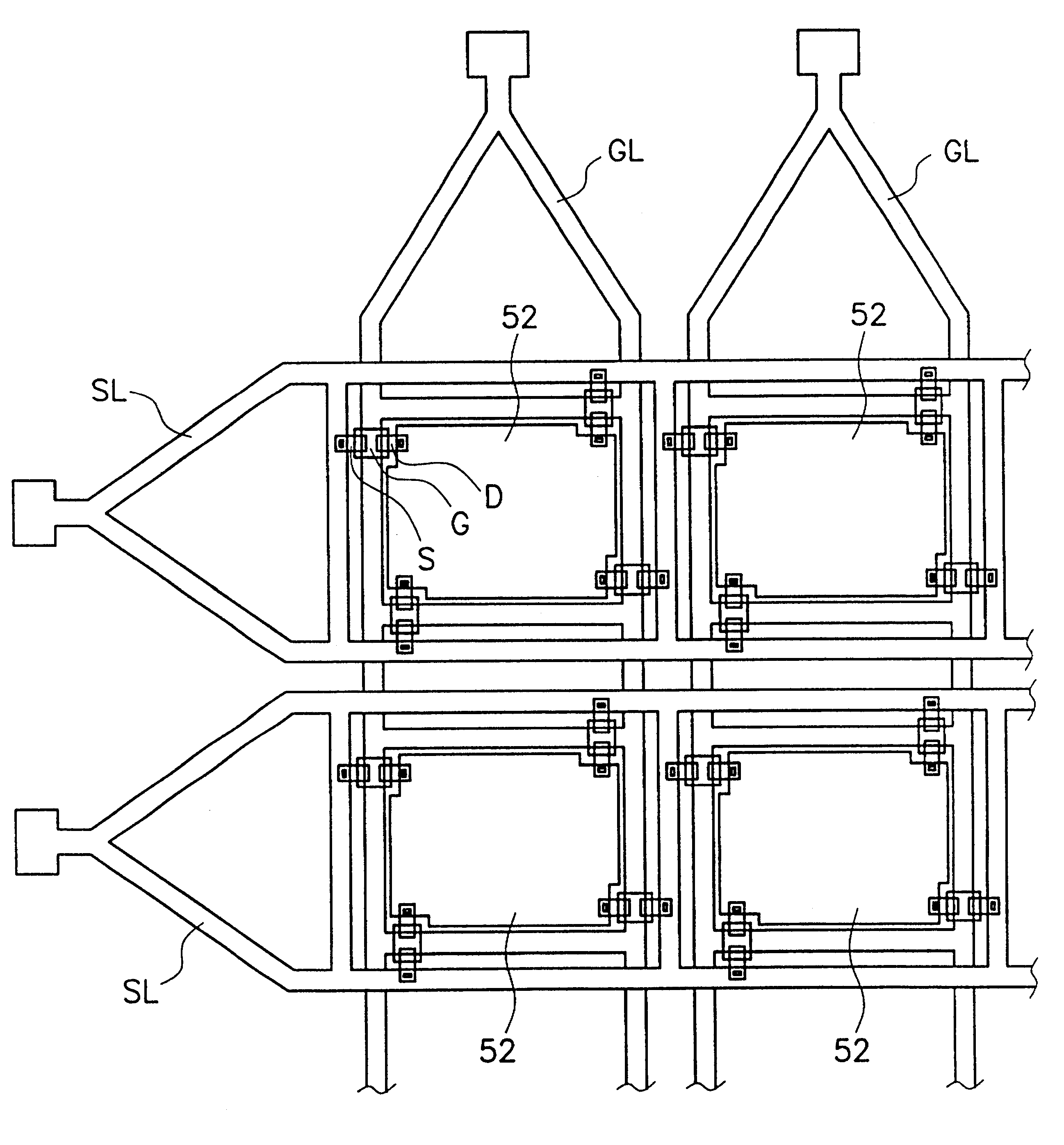
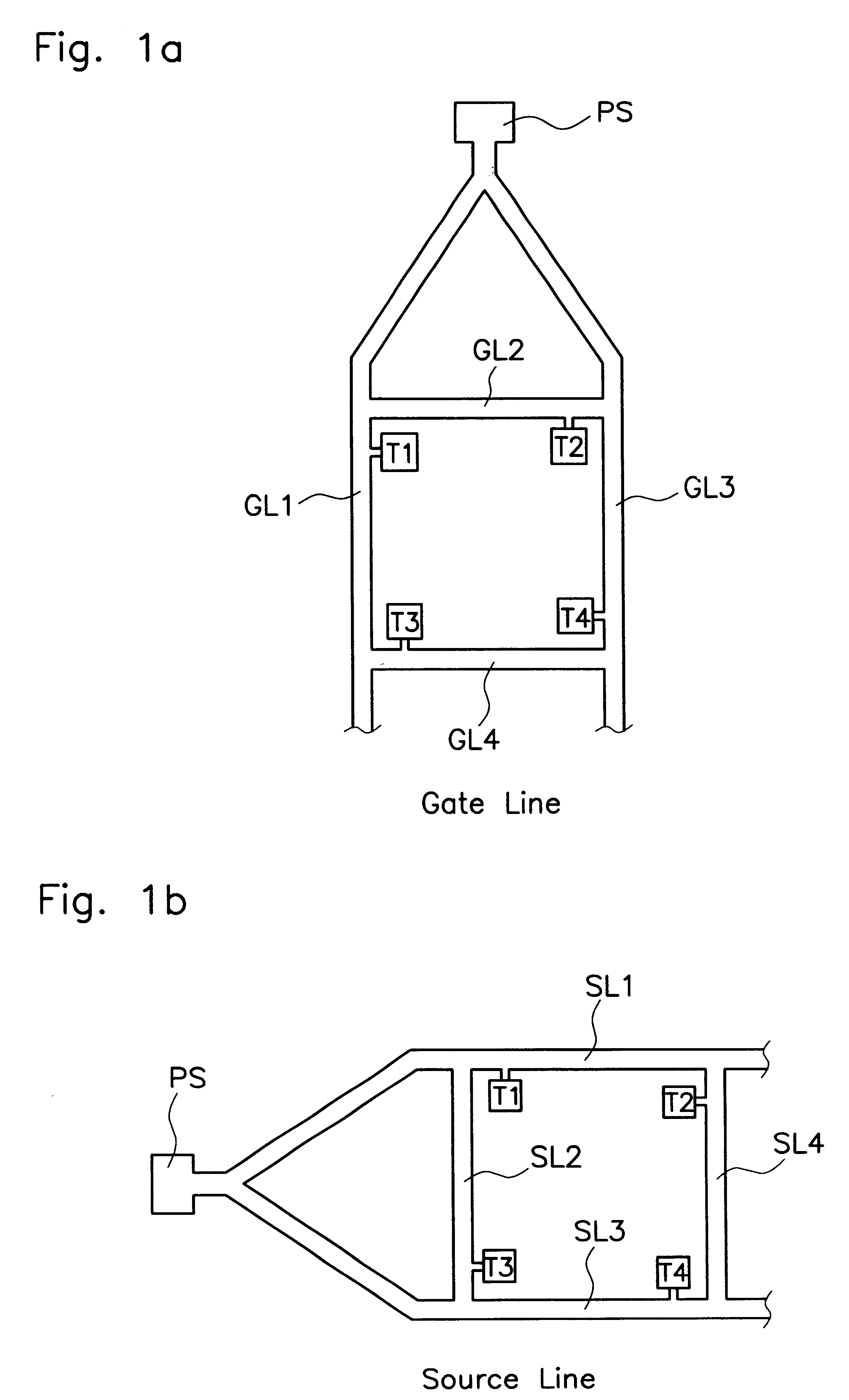
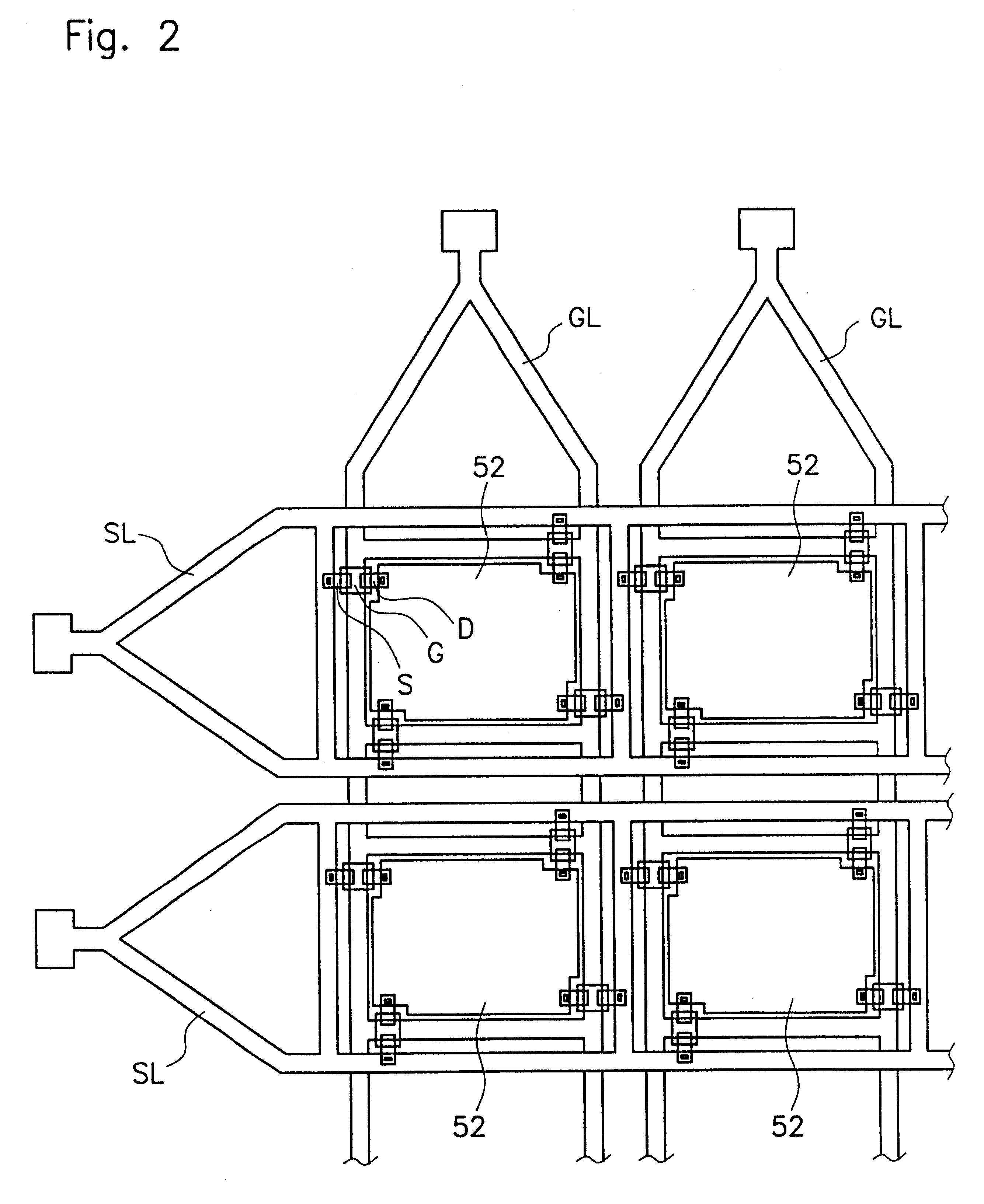
FIGS. 1a and 1b are views separately showing a layout of a line pattern for a thin flim transistor liquid crystal display (LCD) according to the present invention.

Referring to FIG. 1a, a gate line GL defined as a primary line for receiving a signal from a drive IC (not shown) is formed in a lattice shape having two vertical sides GL1 and GL3 and two horizontal sides GL2 and GL4 per a unit pixel electrode by first branching a pattern base portion PS into a right signal line and a left signal line which are spaced by a certain interval and run in parallel with each other, and then connecting the right line and left line with horizontal signal lines, one above and one below the unit pixel electrode.

As shown in FIG. 1b a source line SL serving as a se...


PUM

PropertyMeasurementUnit
dielectric anisotropyaaaaaaaaaa
twisted angleaaaaaaaaaa
defectaaaaaaaaaa

Abstract

A thin film transistor liquid crystal display according to the present invention provides against cut-off of lines for supplying a predetermined "ON'- or "OFF'-signal to thin film transistors and improves "ON'-current characteristic of the thin film transistors arranged in parallel. The thin film transistor liquid crystal display comprises primary lines and secondary lines to supply scanning signals and data signals respectively wherein each of said primary and secondary lines are branched and a thin film transistor is electrically coupled to each of the branched lines such that at least two transistors are turned on and off simultaneously when one of primary lines and one of secondary lines are applied with scanning signals and data signals respectively. Particularly, the primary and secondary lines are patterned in a trapezoid shape to define a lattice having two vertical sides and two horizontal sides for a unit pixel electrode.

Description

1 Field of the InventionThe present invention relates to a thin film transistor liquid crystal display and, more particularly, to a line lay-out pattern of a thin film transistor liquid crystal display capable of providing against cut-off of lines for supplying a predetermined `ON`- or `OFF`-signal to thin film transistors and improving `ON`-current characteristic of the thin film transistors arranged in a parallel.2 Description of the Prior ArtAs well-known, such a liquid crystal display (LCD) device is a typical display that, depending on the dielectric anisotropy feature of liquid crystal materials, controls the amount of light to be penetrated so as to depict image pixels on a screen. Profitably, such a LCD device is employed in a lap-top computer, a word processor, a portable television set and so on.In general, the LCD device may be fabricated in a simple matrix structure in which two strip-shaped electrodes are intersectionally formed in a matrix manner and, thus, the arrange...

Claims


Application Information

Patent Timeline
Patent Type & Authority Patents(United States)
IPC IPC(8): G02F1/13G02F1/1362G02F1/1345H01L29/786G02F1/1343G02F1/136G02F1/1368
CPCG02F1/13624G02F1/1345G02F1/1343G02F1/136
Inventor KIM, BYUNG-HEEKIM, SUN HWAKANG, SEUNG GONSHIN, HYUN EOKCHOI, YOUNG IL
Owner SAMSUNG DISPLAY CO LTD
Why Eureka
Try Eureka