Cleaning with liquified gas and megasonics

a technology of liquified gas and megasonics, applied in the direction of cleaning with liquids, cleaning processes and utensils, chemistry apparatus and processes, etc., can solve the problems of component failure, high cost, and high cost of electronic components

Inactive Publication Date: 2002-02-05
IBM CORP
View PDF16 Cites 48 Cited by
  • Summary
  • Abstract
  • Description
  • Claims
  • Application Information

AI Technical Summary

Benefits of technology

megasonic energy forming means associated with the distributor means to energize the liquefied gas held in the distributor means;

Problems solved by technology

The fabrication of electronic components such as integrated circuit semiconductors is very exacting and complex and requires a number of processing steps requiring extreme precision to form the desired circuit pattern on the component substrate.
Contamination of the semiconductor substrate in the form of particles and / or films on the substrate may cause short circuits, open circuits and other defects which can cause the component to fail and / or adversely affect the performance of the component.
For example, an individual particle as small as 100 angstroms in diameter can result in a killer defect in a modern microcircuit electronic component.
Unfortunately, wafer contamination is still a problem in the semiconductor fabrication industry and as the industry advances and technology is being developed to form smaller and more complex circuits, a more effective and efficient cleaning method is required to produce semiconductor components.

Method used


Image

  • Cleaning with liquified gas and megasonics
  • Cleaning with liquified gas and megasonics

Examples


Embodiment Construction

)

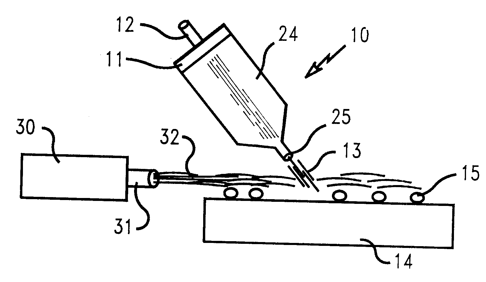
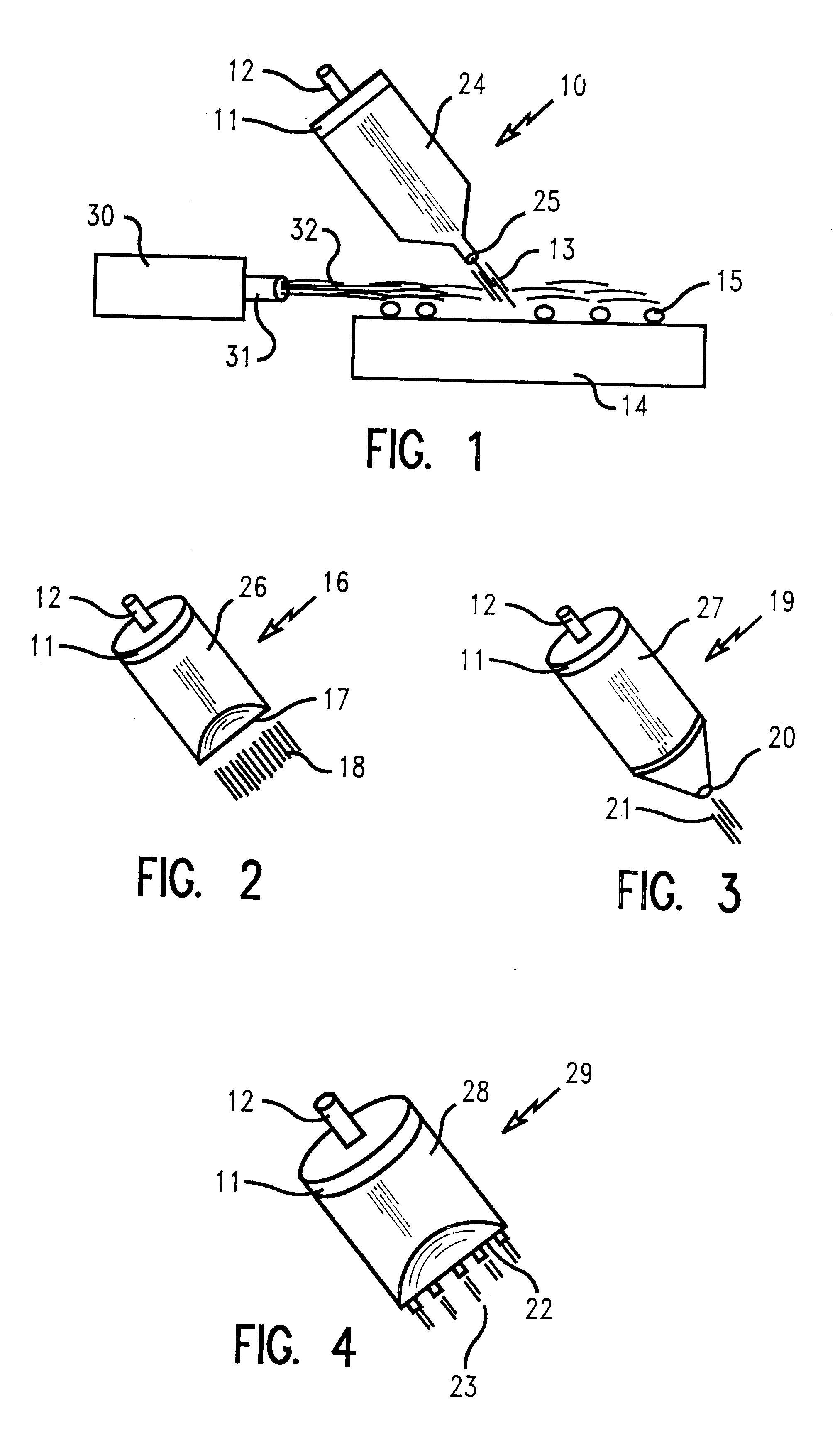
In describing the preferred embodiment of the present invention, reference will be made herein to FIGS. 1-4 of the drawings in which like numerals refer to like features of the invention. Features of the invention are not necessarily shown to scale in the drawings.

The present invention is applicable to cleaning processes for cleaning a wide variety of substrates such as circuit boards, medical instruments and optical lenses and in particular electronic component substrates such as semiconductor wafers used in the fabrication of integrated circuits. Contaminant materials which may be removed from substrates in accordance with the present invention include, but are not limited to, oil, grease, lubricants, solder flux residues, photoresist, particulates comprising inorganic or organic materials, adhesive residues, plasticizers, unreacted monomers, dyes, and dielectric fluids. Typical substrates from which contaminants may be removed by the present process include, but are not limited ...


PUM

PropertyMeasurementUnit
frequencyaaaaaaaaaa
widthsaaaaaaaaaa
diameteraaaaaaaaaa

Abstract

An apparatus and method are provided for cleaning (removing) contaminating particles and/or films from substrate surfaces such as semiconductor wafers during the fabrication process for making electronic components. The method and apparatus use a liquified gas contained in a distributor which has been energized with megasonic energy in the distributor and the energized liquefied gas directed as a stream against the surface to be cleaned from an outlet distribution nozzle of the distributor. The stream is preferably impinged on the substrate surface at an acute angle. The preferred liquified gas is carbon dioxide.

Description

1. Field of the InventionThis invention relates generally to the fabrication of electronic components such as integrated circuit semiconductors and, in particular, to the cleaning of contaminates from the surface of substrates such as semiconductor wafers used to make the electronic component.2. Description of Related ArtThe fabrication of electronic components such as integrated circuit semiconductors is very exacting and complex and requires a number of processing steps requiring extreme precision to form the desired circuit pattern on the component substrate. Typical semiconductor devices now have circuit line widths typically less than 1 micron with close spacing of the lines and via interconnections. Contamination of the semiconductor substrate in the form of particles and / or films on the substrate may cause short circuits, open circuits and other defects which can cause the component to fail and / or adversely affect the performance of the component. For example, an individual p...

Claims


Application Information

Patent Timeline
Patent Type & Authority Patents(United States)
IPC IPC(8): B08B3/02B08B7/00H01L21/00
CPCB08B3/02B08B7/0021H01L21/67051Y10S134/902B08B2203/0288
Inventor KIM, BEN
Owner IBM CORP
Why Eureka
Try Eureka