Supercharge Your Innovation With Domain-Expert AI Agents!

Method of producing semiconductor device and configuration thereof, and lead frame used in said method

a semiconductor device and lead frame technology, applied in semiconductor devices, semiconductor/solid-state device details, electrical apparatus, etc., can solve the problems of high heat generation, difficult to apply the device to high-output power transistors, and difficult to apply the device to high-frequency transistors or the lik

Inactive Publication Date: 2002-04-16
MITSUBISHI ELECTRIC CORP
View PDF8 Cites 5 Cited by
  • Summary
  • Abstract
  • Description
  • Claims
  • Application Information

AI Technical Summary

Benefits of technology

This approach simplifies production, reduces costs, enhances heat dissipation, and improves high-frequency performance by allowing direct connection to motherboards, reducing size and weight, and increasing bonding strength.

Problems solved by technology

Moreover, because heat generated by the semiconductor element 3 is dissipated through the lead 6, it is difficult to apply the device to high-output power transistors which generated much heat.
Because of the relatively long connection between the semiconductor element 3 and a mother board, it is also difficult to apply the device to high-frequency transistors or the like.
However, since production of such a molded transistor requires different lead frames for different specifications as in the prior art and molding with the resin is carried out individually for each semiconductor element, different molding dies must be prepared according to different specifications and therefore the above problems are not solved.
Also the devices are mounted on the mother board by using flat leads according to this prior art technology, but it cannot be applied to devices which generate much heat because of relatively small lead area.

Method used


Image

  • Method of producing semiconductor device and configuration thereof, and lead frame used in said method
  • Method of producing semiconductor device and configuration thereof, and lead frame used in said method
  • Method of producing semiconductor device and configuration thereof, and lead frame used in said method

Examples


embodiment 1

First embodiment of the present invention will now be described below with reference to FIG. 1A through FIG. 3D.

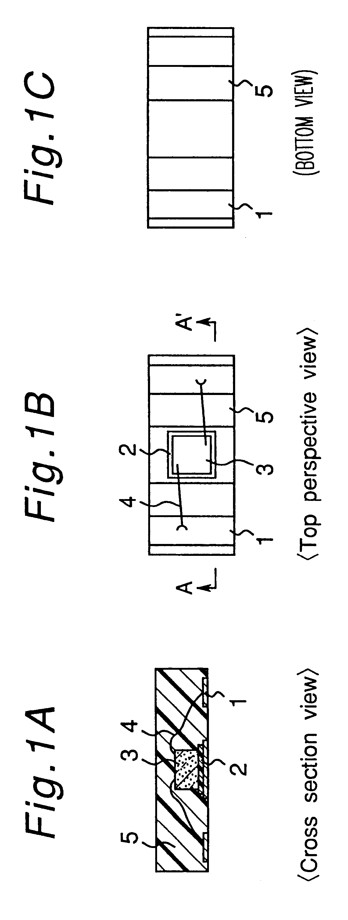
FIGS. 1A-1C show a semiconductor device according to the present invention, with FIG. 1A showing a cross sectional view taken along lines A-A', FIG. 1B showing a top view and FIG. 1C showing a bottom view. In the drawing, numeral 1 denotes an external electrode (wire bond pad), 2 denotes a die bonding material, 3 denotes a semiconductor element, 4 denotes a wire such as gold wire and 5 denotes sealing resin.

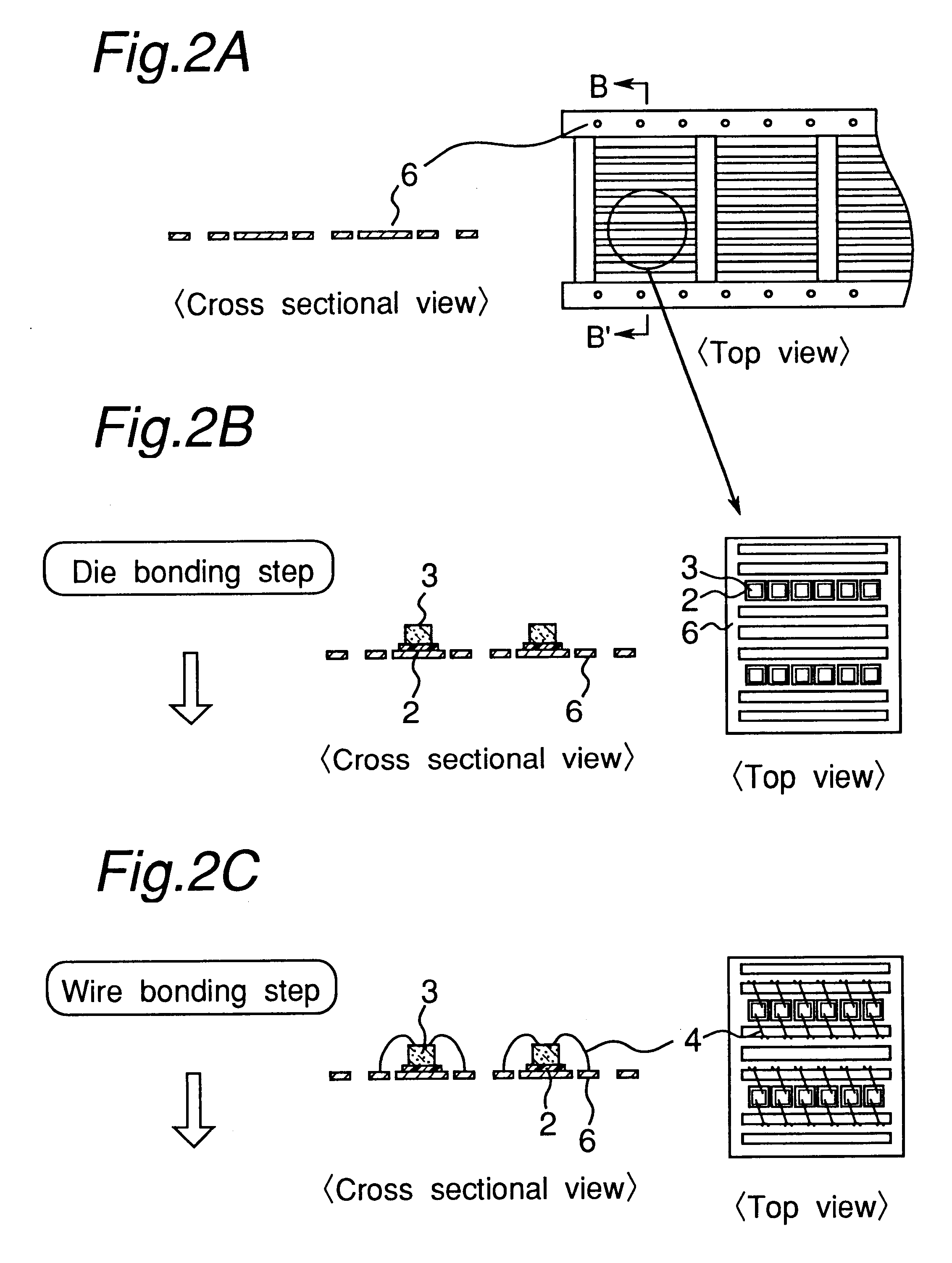
A method of producing the semiconductor device shown in FIGS. 1A-1C will be described below with reference to FIGS. 2A-3D.

First, such a lead frame 6 is prepared as shown in FIG. 2A where a plurality of leads are arranged parallel to each other at intervals. The lead frame 6 is shown in FIG. 2A as a top view on the right and cross sectional view taken along lines B-B' on the left. FIGS. 2A-3D show the top view on the right and cross sectional view of that portion taken a...

embodiment 2

A semiconductor device of another embodiment of the present invention will be described below with reference to FIGS. 4A-6B.

FIGS. 4A and 4B show the semiconductor device having a plurality of recesses on the top surface of the lead, with a top view (perspective view) on the right (FIG. 4A) and a cross sectional view of the portion taken along lines E-E' on the left (FIG. 4B). In the drawing, the same reference numerals as those in FIGS. 1A-1C denote the identical or corresponding parts. FIGS. 4A and 4B show such a structure that is cut off through a recess provided on the top surface of the lead 1 wherever dicing is done.

FIG. 5A and 5B show the semiconductor device having uneven surface made on the side of the lead, with a top view (perspective view) on the right (FIG. 5A) and a cross sectional view of the portion taken along lines E-E' on the left (FIG. 5B). In the drawing, same reference numerals as those in FIGS. 1A-1C denote the identical or corresponding parts. FIGS. 5A and 5B ...

embodiment 3

A semiconductor device of another embodiment of the present invention will be described below with reference to FIGS. 7A-8D.

FIGS. 7A and 7B show the semiconductor device having a plurality of recesses formed on the back surface of the lead, with a top view (perspective view) on the right (FIG. 7A) and a cross sectional view of the portion taken along lines E-E' on the left (FIG. 7B). In the drawing, same reference numerals as those in FIGS. 1A-1C denote the identical or corresponding parts. FIG. 7 shows such a structure that is cut off through a recess provided on the back surface of the lead 1 wherever dicing is done.

FIGS. 8A-8D are schematic diagrams showing a case of mounting the semiconductor device of this embodiment on the mother board 17. In the drawing, numeral 26 denotes solder paste which has been transferred, 27 denotes an electrode pad formed on the mother board, 15 denotes a solder patch formed by reflowing of the solder paste and 23 denotes a solder fillet formed on th...


PUM


Abstract

Providing a method of producing a semiconductor device wherein semiconductor element are sealed with a resin by using the same lead and other means regardless of the specifications of the semiconductor elements, and a semiconductor device which can be reduced in size and weight and has good heat dissipation performance and high-frequency performance.The semiconductor devices can be produced by mounting a plurality of the semiconductor elements on the lead frame having leads disposed substantially parallel to each other, sealing the whole with a resin, and cutting off the individual semiconductor devices.

Description

1. Field of the InventionThe present invention relates to a method of producing a semiconductor device and a configuration thereof. More particularly, it relates to a method of producing a resin-sealed semiconductor device and a configuration thereof which make it possible to decrease the size, thickness, weight and cost of the device.2. Description of the Related ArtFIGS. 15A and 15B show a gull-wing type semiconductor device with the configuration of the prior art, FIG. 15A being a cross sectional view thereof and FIG. 15B being a top view thereof.A semiconductor device of this configuration is generally produced in such steps as shown in FIG. 16, in a procedure described below. A semiconductor element 3 is bonded by means of a die bonding material 2 on an island 24 of a lead frame 6 which has the islands 24 and leads 1 as shown in FIG. 17. Then after connecting an inner lead section of the lead 1 surrounding the island 24 to an electrode pad located on the semiconductor element 3...

Claims


Application Information

Patent Timeline
Patent Type & Authority Patents(United States)
IPC IPC(8): H01L21/56H01L21/02H01L23/28H01L23/31H01L23/48
CPCH01L21/565H01L23/3107H01L24/97H01L2224/85444H01L2224/48091H01L2224/48247H01L2224/73265H01L2224/92247H01L2924/01057H01L2924/01078H01L2924/01079H01L24/45H01L2924/01029H01L2924/15747H01L2924/07802H01L24/48H01L2224/32245H01L2224/97H01L2224/45144H01L2924/00014H01L2924/00H01L2924/00012H01L2924/351H01L2224/48644H01L2924/12042H01L24/73H01L2924/181H01L2224/48465H01L21/50
Inventor OHGIYAMA, KENJIFUJIHARA, TERUHISAUEDA, TAMOTSU
Owner MITSUBISHI ELECTRIC CORP
Features
  • R&D
  • Intellectual Property
  • Life Sciences
  • Materials
  • Tech Scout
  • Unparalleled Data Quality
  • Higher Quality Content
  • 60% Fewer Hallucinations
Learn More