Light emitting device and method for manufacturing the same

a light emitting device and light technology, applied in the direction of semiconductor/solid-state device manufacturing, semiconductor devices, electrical devices, etc., can solve the problems of inability to obtain inability to form a thin mold for the thermoplastic resin based composite material, and inability to achieve the necessary strength of molding for releasing, etc., to achieve stable light emitting property, efficient production of light emitting devices, and stable light emitting properties

Active Publication Date: 2010-12-16
NICHIA CORP
View PDF6 Cites 116 Cited by
  • Summary
  • Abstract
  • Description
  • Claims
  • Application Information

AI Technical Summary

Benefits of technology

[0028]According to the above-mentioned steps of the manufacturing method of the light emitting device, an upper mold on which the same shaped spaces as the recess, the periphery, and the bottom of the first resin forming body are beforehand formed, and a lower mold that corresponds to the upper mold, are used in the steps. Accordingly, a thick shaped periphery that works as a casing of the light emitting device and a thin shaped bottom that forms a bottom of the recess of the first resin forming body, can be produced at the same time. Therefore, a step that is needed for a conventional light emitting device is not needed

Problems solved by technology

Hereby, a problem that the lead frames 320 and 330 lift is caused.
In general, fluidity of the thermoplastic resin based composite material is inferior to that of the thermosetting resin based composite material.
Therefore, it is difficult to form a molding in a thin shape for the thermoplastic resin based composite material.
However, in this case, it is impossible to obtain a sufficient strength of the molding needed for releasing in an injection molding process.
Hereby, there is a case that chipping of the molding occurs when the molding is taken out from molds.
Further,

Method used


Image

  • Light emitting device and method for manufacturing the same
  • Light emitting device and method for manufacturing the same
  • Light emitting device and method for manufacturing the same

Examples


first embodiment

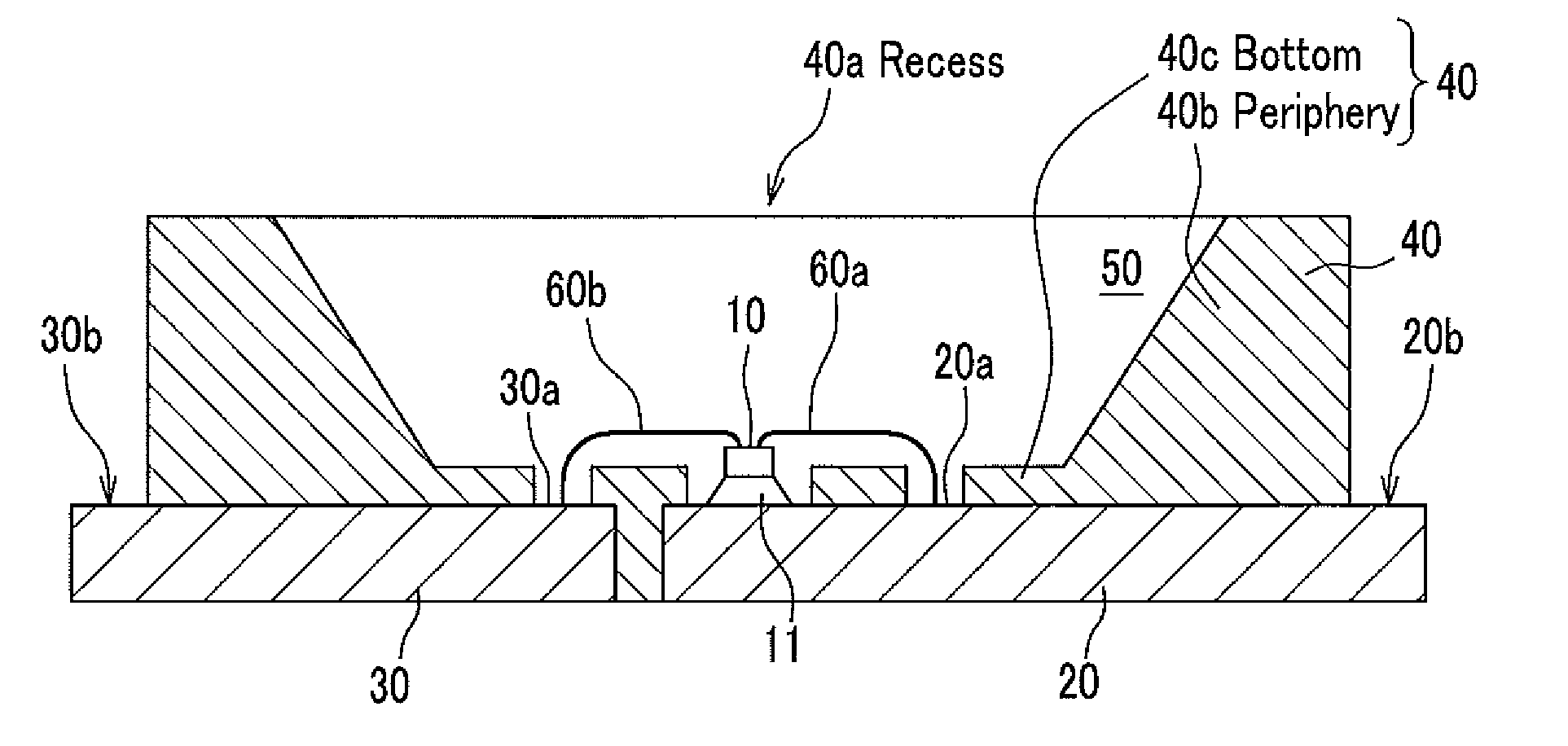
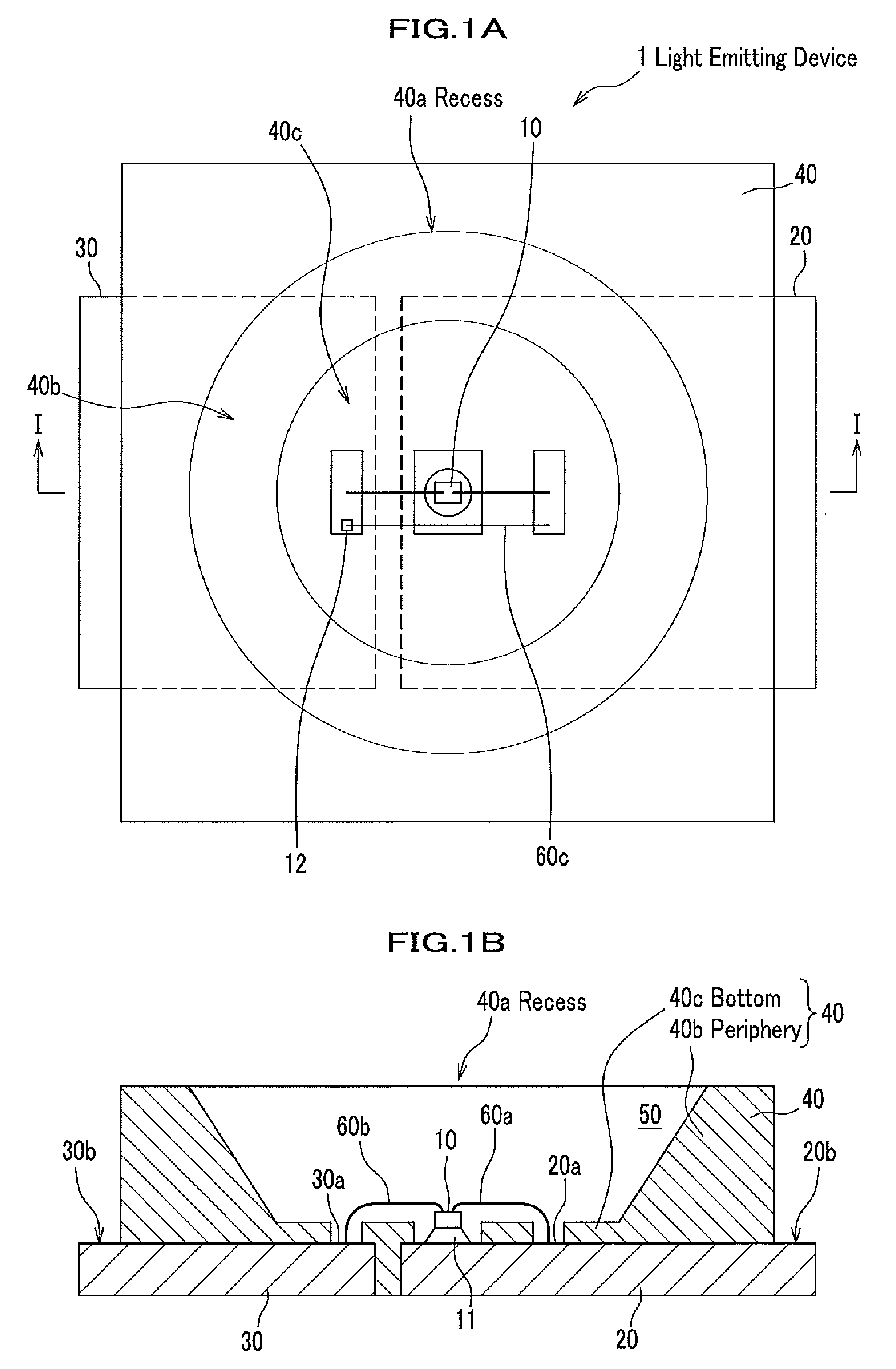
[0043][Construction of Light Emitting Device]

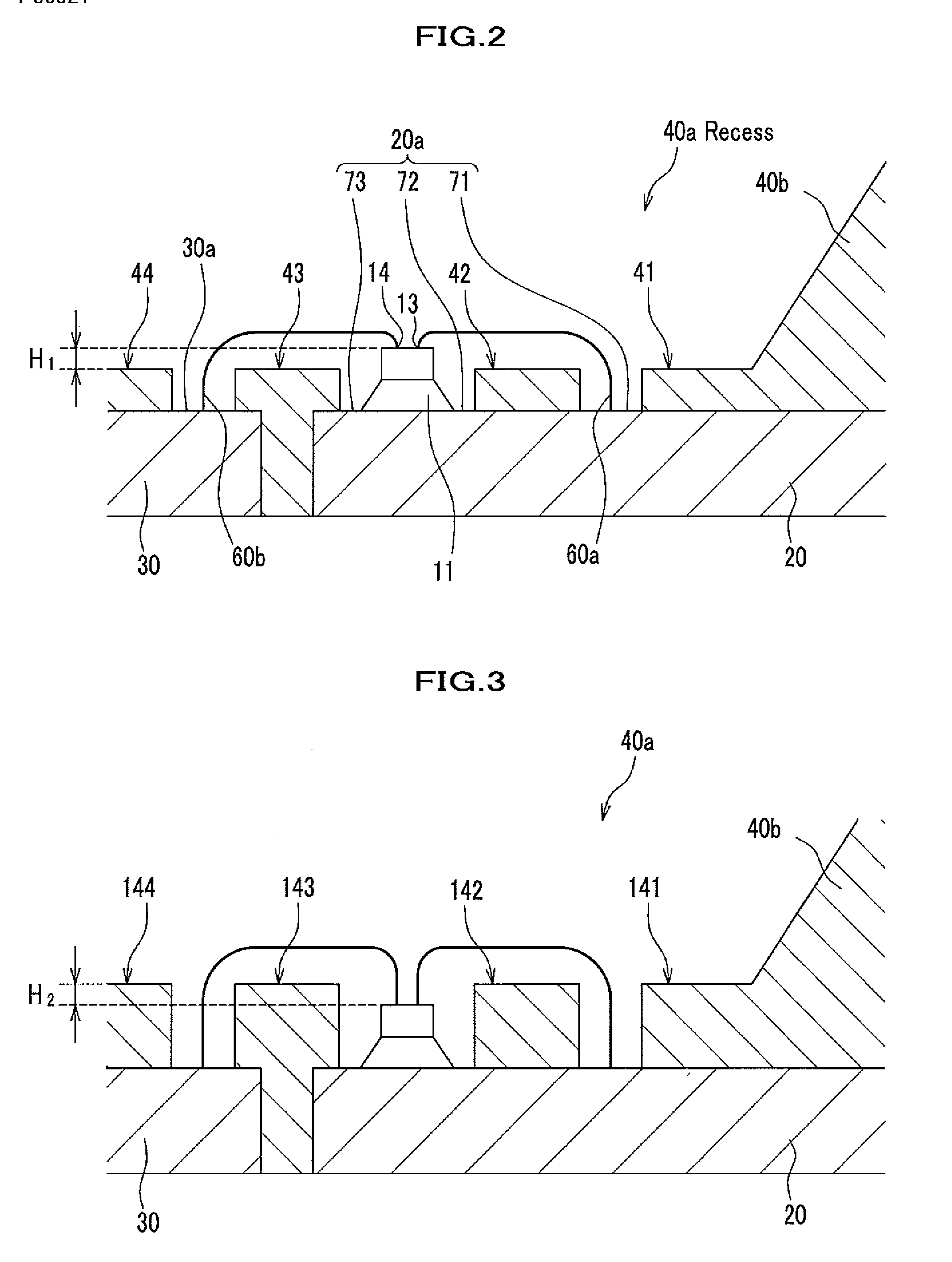
[0044]FIGS. 1A and 1B are schematic diagrams showing a construction of the light emitting device of the first embodiment of the present invention. FIG. 1A is a plan view of the light emitting diagram observed from a main light emitting surface side. FIG. 1B is a I-I line cross-sectional diagram of FIG. 1A. FIG. 2 is a magnified cross sectional diagram of a portion of FIG. 1B, in the light emitting device.

[0045]A light emitting device 1 of the first embodiment comprises, a light emitting element 10, a first lead frame 20, a second lead frame 30, a first resin forming body 40, and a second resin forming body 50. In the light emitting device of the present invention, a surface side on which the light emitting element 10 is mounted is called a main surface side, and the opposite side is named rear surface side. The first and the second lead frames 20 and 30 are electrically connected to the light emitting element 10. The first resin forming b...

second embodiment

[0088]FIG. 6 is a cross-sectional diagram schematically showing a construction of the light emitting device of the third embodiment of the present invention. The light emitting device of the third embodiment has the same construction as the first embodiment except for a difference in a shape of the bottom 40c of the first resin forming body 40. Thus, the same numbers are used in FIG. 6 as in FIG. 2 and additional explanations will be omitted. As shown in FIG. 6, a bottom 40c (coverings 41, 43, and 44) of a first resin forming body 40 of the third embodiment, covers surfaces of first and second lead frames 20 and 30 except for mounting regions 73 and 74 of the light emitting element 10, and a mounting region of a wire 60a and a mounting region of a wire 60b (second inner lead 30a), and an extended part 41a is formed with the covering 41. That is, at the bottom 40c (coverings 41, 43, and 44) of the first resin forming body 40 shown in FIG. 6, a mounting region 71 for the wire 60a that...

forth embodiment

[0090]FIGS. 7A and 7B are schematic diagrams showing a construction of the light emitting device of the fourth embodiment of the present invention. FIG. 7A is a plan view of the light emitting device observed from a main light emitting surface side. FIG. 7B is a VII-VII line cross-sectional diagram of FIG. 7A. The light emitting device 1C of the forth embodiment further includes a base 80 in addition to first and second lead frames 20 and 30. The light emitting device 1C of the fourth embodiment including the base 80, has the same construction as the light emitting device 1 of the first embodiment except for a difference in shapes of the first lead and the second lead frames 20 and 30. Therefore, the same numbers are used in FIGS. 7A and 7B as in FIGS. 1A and 1B, and similar explanations will be omitted. The base 80 is provided between the first lead frame 20 and the second lead frame 30. The light emitting element 10 is mounted on the base 80. A shape of the base 80 is rectangular ...


PUM


Abstract

A light emitting device, which can be efficiently manufactured and maintain a stable light emitting property for a long period, is provided. The light emitting device comprises a first resin forming body including a periphery that forms a recess to house a light emitting element and a bottom that forms a bottom portion of the recess, and a second resin forming body which covers the light emitting element. The first resin forming body is composed of a thermosetting epoxy resin composite whose essential component is an epoxy resin. The bottom covers surfaces of lead frames excluding mounting regions of the light emitting element and wires. A thickness of the bottom is formed thinner than a thickness from the surface of the lead frames to a leading end of the light emitting element.

Description

CROSS REFERENCE TO RELATED APPLICATIONS[0001]This application claims the foreign priority benefit under Title 35, United State Code, 119 (a)-(d) of Japanese Patent Application No. 2006-353669, filed on Dec. 28, 2006 in the Japan Patent Office, the disclosure of which is herein incorporated by reference in its entirety.BACKGROUND OF THE INVENTION[0002]1. Field of the Invention[0003]The present invention relates to alight emitting device and a method for manufacturing the light emitting device.[0004]Particularly, the present invention relates to a light emitting device having a high output power and reliability, which is used for an illumination apparatus, a backlight, a light emitting apparatus mounted on a vehicle, a display, an auxiliary light source for moving image illumination, and other general industrial and consumer light sources, and a method for manufacturing the light emitting device.[0005]2. Description of Related Art[0006]A light emitting device using a light emitting el...

Claims


Application Information

Patent Timeline
IPC IPC(8): H01L33/62H01L33/48H01L33/60
CPCH01L33/486H01L33/60H01L2924/3025H01L2224/73265H01L2224/48247H01L2224/48091H01L2224/32245H01L2224/45144H01L33/62H01L2924/00014H01L2924/00
Inventor HAYASHI, MASAKI
Owner NICHIA CORP
Why Eureka
Try Eureka