

Copper circuit junction substrate and method of producing the same
a technology of copper circuit junction and substrate, which is applied in the direction of metal-working apparatus, solid-state devices, metal-patterned materials, etc., can solve the problems of low thermal expansion coefficient low compatibility of copper and substrate, and high cost of copper circuit junction, etc., to achieve higher thermal stress relaxation effect, higher thermal stress concentration, and high reliability
- Summary
- Abstract
- Description
- Claims
- Application Information
AI Technical Summary
Benefits of technology
Problems solved by technology
Method used
Image

Examples
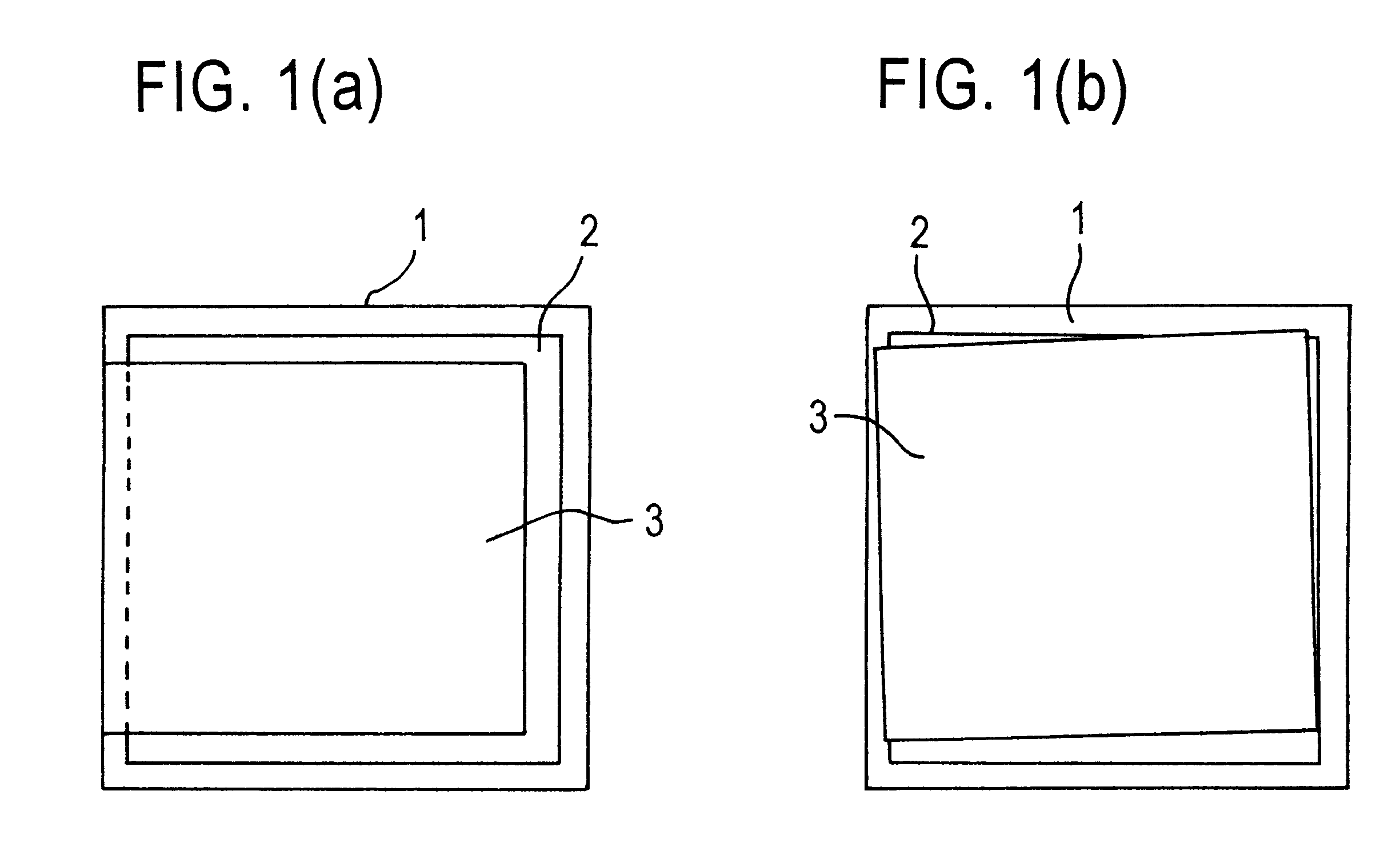
example 1
An AlN powder, an Si.sub.3 N.sub.4 powder, and Al.sub.2 O.sub.3 powder each having an average particle diameter of 1 .mu.m were provided as main component powders. Further, a Y.sub.2 O.sub.3 powder having an average particle diameter of 0.6 .mu.m and a CaO powder having an average particle diameter of 0.3 .mu.m were provided as sintering aid powders. 97% by weight of one of the three kinds of main component powders and a sintering aid powder of a combination of 1.5% by weight of the Y.sub.2 O.sub.3 powder with 1.5% by weight of the CaO powder were weighed and mixed together in an ethanol solvent in a ball mill for 24 hr. Thus, three kinds of mixed powders, that is, an AlN mixed powder containing Y.sub.2 O.sub.3 --CaO as a sintering aid, an Si.sub.3 N.sub.4 mixed powder containing Y.sub.2 O.sub.3 --CaO as a sintering aid, and an Al.sub.2 O.sub.3 mixed powder containing Y.sub.2 O.sub.3 --CaO as a sintering aid were obtained. 10 parts by weight of PVB (polyvinyl butyral) as a binder wa...
example 2
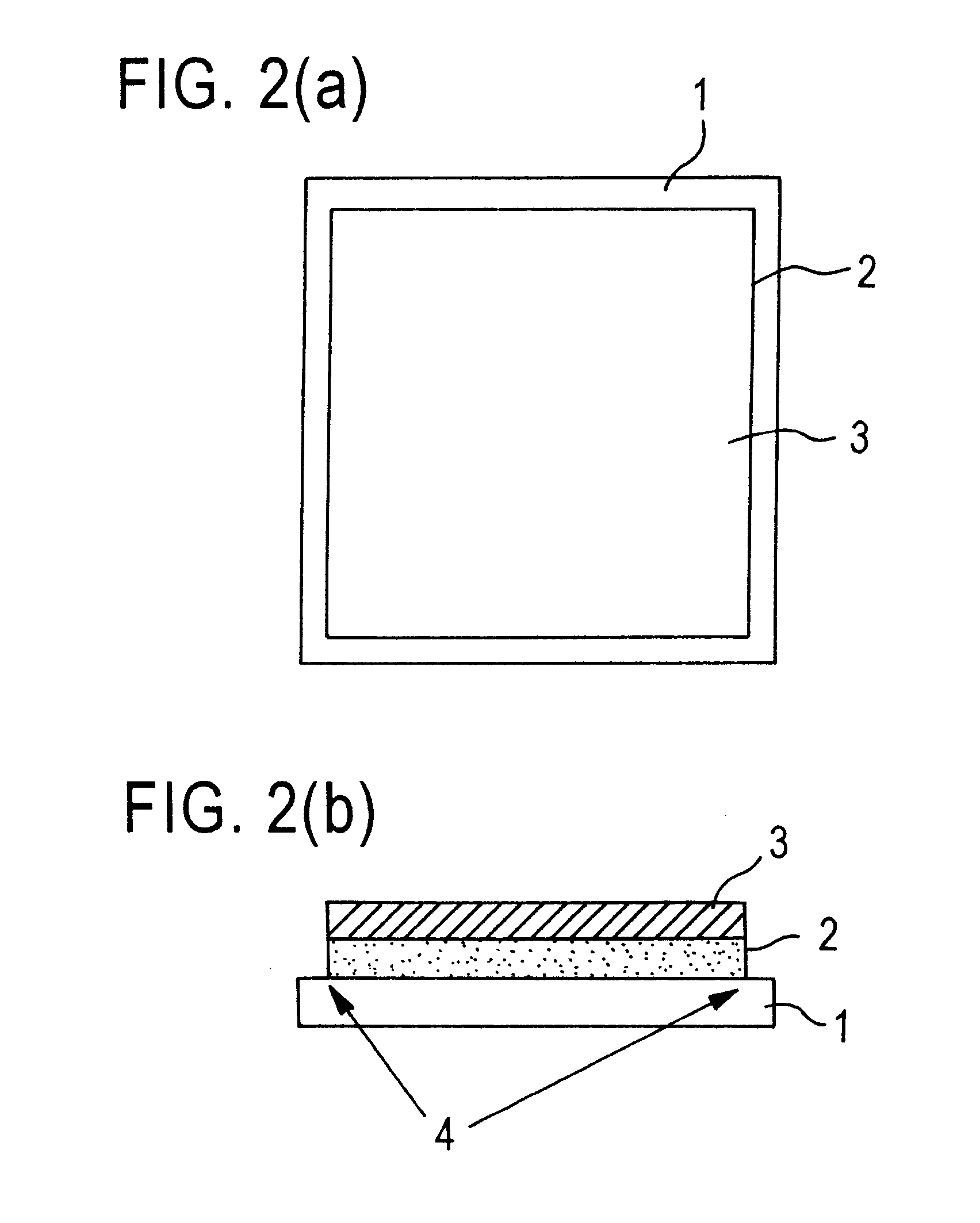
Three kinds of compacts of an AlN-based material, an Si.sub.3 N.sub.4 -based material, and an Al.sub.2 O.sub.3 -based material (except for high-thermal conductivity silicon nitride ceramic) were prepared using the same starting materials, mixing formulation, and mixing / molding procedures as described in Example 1. Half of these compacts were selected, and a high-melting metal paste comprising a high-melting metal W as a main component and an SiO.sub.2 --CaO--B.sub.2 O.sub.3 glass was applied by printing on one main plane of the compacts, followed by firing in a nitrogen atmosphere at 1,600.degree. C. for 5 hr to sinter each compact body and at the same time to sinter the high-melting metal paste. In this case, as with Example 1, the high-melting metallizing layer was formed over substantially the whole surface of the ceramic substrate. The weight ratio of the high-melting metal in the high-melting metallizing layer to the glass was 85:15. The glass had a composition comprising, in t...
example 3
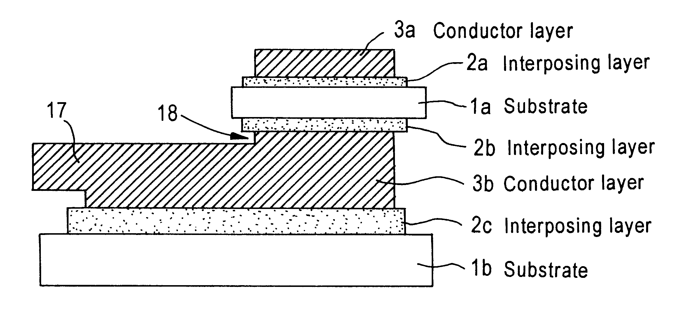
Four kinds of ceramic substrates of the same materials and combinations as described in Example 1 were prepared (including high-thermal conductivity silicon nitride ceramic substrate samples A and B having a smaller thickness of 0.5 mm which is different from the thickness of the other three kinds of substrates as provided in Example 1). As with Example 1, the main plane of the interposing layer had substantially the same shape as the main plane of the substrate. The composition, thickness and the like of the interposing layer were as given in Table 3. For the high-thermal conductivity silicon nitride ceramic materials A and B, circuit boards having a interposing layer / conductor layer structure according to sample 46 in Table 3 were prepared. When the interposing layer consisted of the brazing material layer alone, the joining interposing layer and the conductor layer were formed in the same manner as in Example 1, when the interposing layer comprised a first layer of a high-melting...
PUM
| Property | Measurement | Unit |
|---|---|---|
| Length | aaaaa | aaaaa |
| Angle | aaaaa | aaaaa |
| Angle | aaaaa | aaaaa |
Abstract
Description
Claims
Application Information