Semiconductor power converting apparatus

a technology of semiconductor power, which is applied in the direction of power conversion system, electronic switching, pulse technique, etc., can solve the problems of reducing the converter efficiency, increasing the cost of the semiconductor power converting apparatus, and reducing the efficiency of the converter

Inactive Publication Date: 2002-04-30
HITACHI LTD
View PDF8 Cites 59 Cited by
  • Summary
  • Abstract
  • Description
  • Claims
  • Application Information

AI Technical Summary

Benefits of technology

Furthermore, a semiconductor power converting apparatus, according to the present invention, is featured by that either a zener diode or a voltage source is inserted in series to a voltage dividing resistor which divides a voltage appearing between an emitter and a collector of a semiconductor element so as to increase a changing ratio of a gate voltage with respect to the voltage between the emitter and the collector of this semiconductor element while a peak voltage is suppressed. As a result, the peak voltage suppressing effect is improved. With employment of the circuit arrangement, the peak voltage suppressing operation when the semiconductor element is turned OFF can be effectively carried out.
Furthermore, a semiconductor power converting apparatus, according to the present invention, is featured by that a circuit constituted by either a capacitor or a switch is connected in parallel to a portion of a voltage dividing resistor which divides a voltage appearing between a collector of a semiconductor element and an emitter thereof, and such a device is provided which changes a voltage dividing ratio in such a manner that a relationship between the gate voltage and the collector potential can be continuously, or stepwise changed, and rising of the collector potential is commenced. Then, the voltage dividing device can suppress a peak voltage appearing between the collector and the emitter by changing the setting condition even when dv / dt of the voltage between the collector and the emitter of the semiconductor element is high. With employment of this circuit arrangement, in order to increase the efficiency of the semiconductor power converting apparatus, it is possible to increase the dv / dt of the voltage between the collector and the emitter when the current of the semiconductor element is interrupted. Also, another peak voltage by charging time of the gate capacitance of the semiconductor element can be suppressed even for a high dv / dt occurred other than the current interruption of the semiconductor element.
Furthermore, a semiconductor power converting apparatus, according to the present invention, is featured by employing a device for changing a voltage dividing ratio by way of a timer switch connected in parallel to a portion of a voltage dividing resistor which divides a voltage appearing between a collector of a semiconductor element and an emitter thereof. Then, after the semiconductor element has been turned OFF, the voltage between the collector and the emitter of the semiconductor element is stationally stabilized with respect to the power supply voltage. After a preselected time period has passed, the voltage dividing ratio is changed into a higher value than the power supply voltage, so that the reverse bias can be applied to the gate of the semiconductor element. With employment of this circuit arrangement, a voltage between the collector of the semiconductor element and the emitter thereof after the peak voltage has been suppressed is stabilized to becomes such a voltage obtained by dividing the power supply voltage by a total number of series-connected elements. Thereafter, the reverse bias can be applied to the gate, so that the noise margin may be improved in order that the erroneous ON state never occurs.
Furthermore, a semiconductor power converting apparatus, according to the present invention, is featured by that more than two sets of semiconductor elements are connected in series to each other so as to constitute an arm, the arms are simultaneously turned ON, or OFF. Then, a voltage dividing ratio of a voltage dividing device is set in such a manner that the voltages between the collectors and the emitters of the respective semiconductor elements can be equally shared, so that the voltages between the collectors and the emitters of the series-connected semiconductor elements may be made equal. With employment of this circuit arrangement, in such a semiconductor power converting apparatus that a plurality of series-connected semiconductor elements are simultaneously turned ON or OFF, the peak voltage of the voltage appearing between the collector and the emitter of each of the semiconductor elements series-connected to each other can be suppressed. Also, the stationary voltage stabilizing operation after suppressing the peak voltage is carried out in a highspeed, and the switching frequency of the semiconductor power apparatus converting apparatus is increased. As a result, the power converting efficiency can be increased.

Problems solved by technology

Furthermore, these IGBTs are desirably applied to semiconductor power converting apparatuses having large capacities.
Thus, switching losses of these snubber circuits would reduce the converter efficiency, namely could not be neglected.
Moreover, since the snubber circuits are connected to such a semiconductor power converting apparatus, the cost thereof is increased and this semiconductor power converting apparatus becomes bulky.
This requires time and high cost.
As a result, there are such problems that the higher withstanding voltage of the IGBT cannot be realized, but also the switching loss is increased.
As a consequence, the switching frequency could not be made high.

Method used


Image

  • Semiconductor power converting apparatus
  • Semiconductor power converting apparatus
  • Semiconductor power converting apparatus

Examples


first embodiment

FIG. 1, FIG. 2 and FIG. 3 are diagram for indicating a first embodiment mode of the present invention.

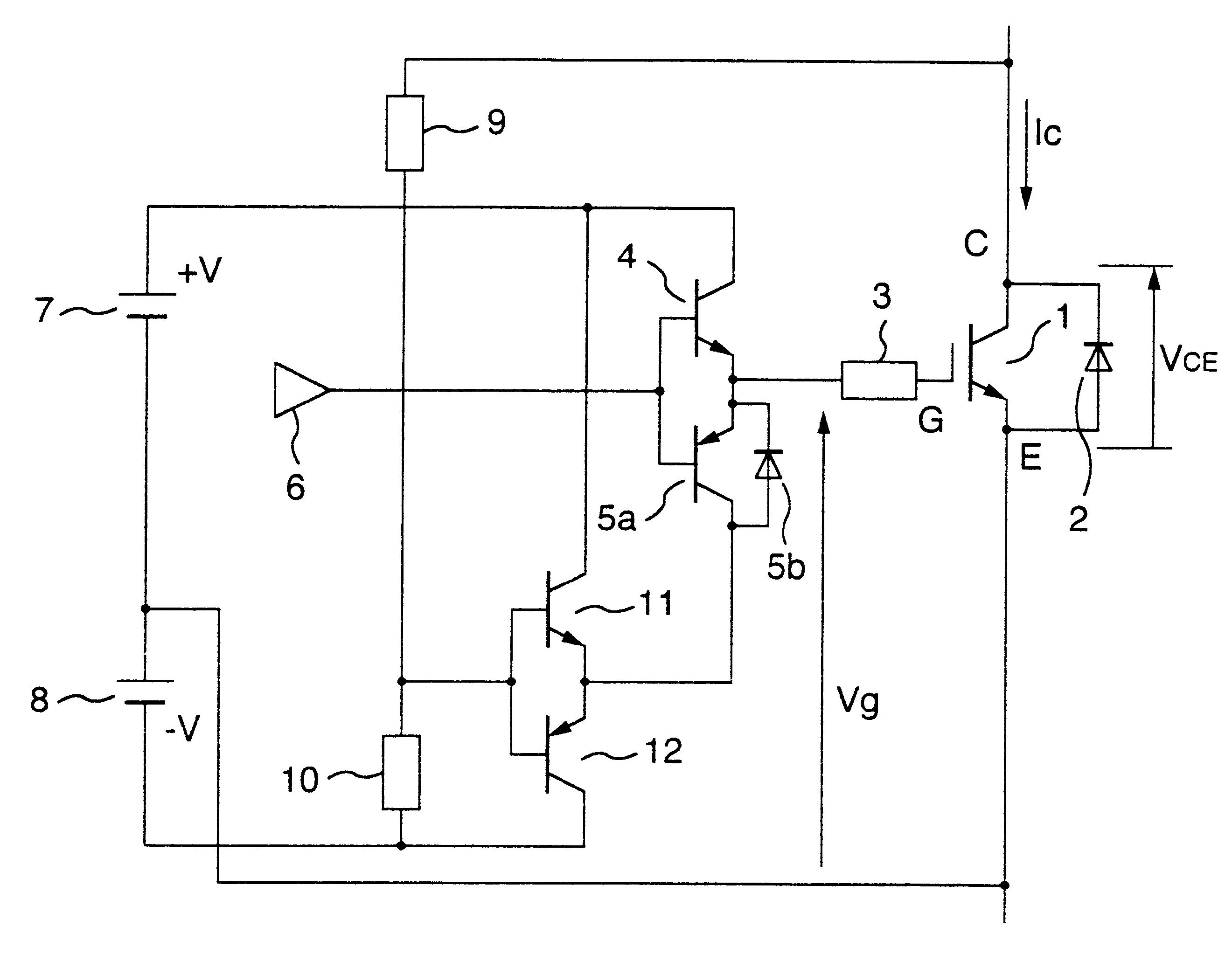
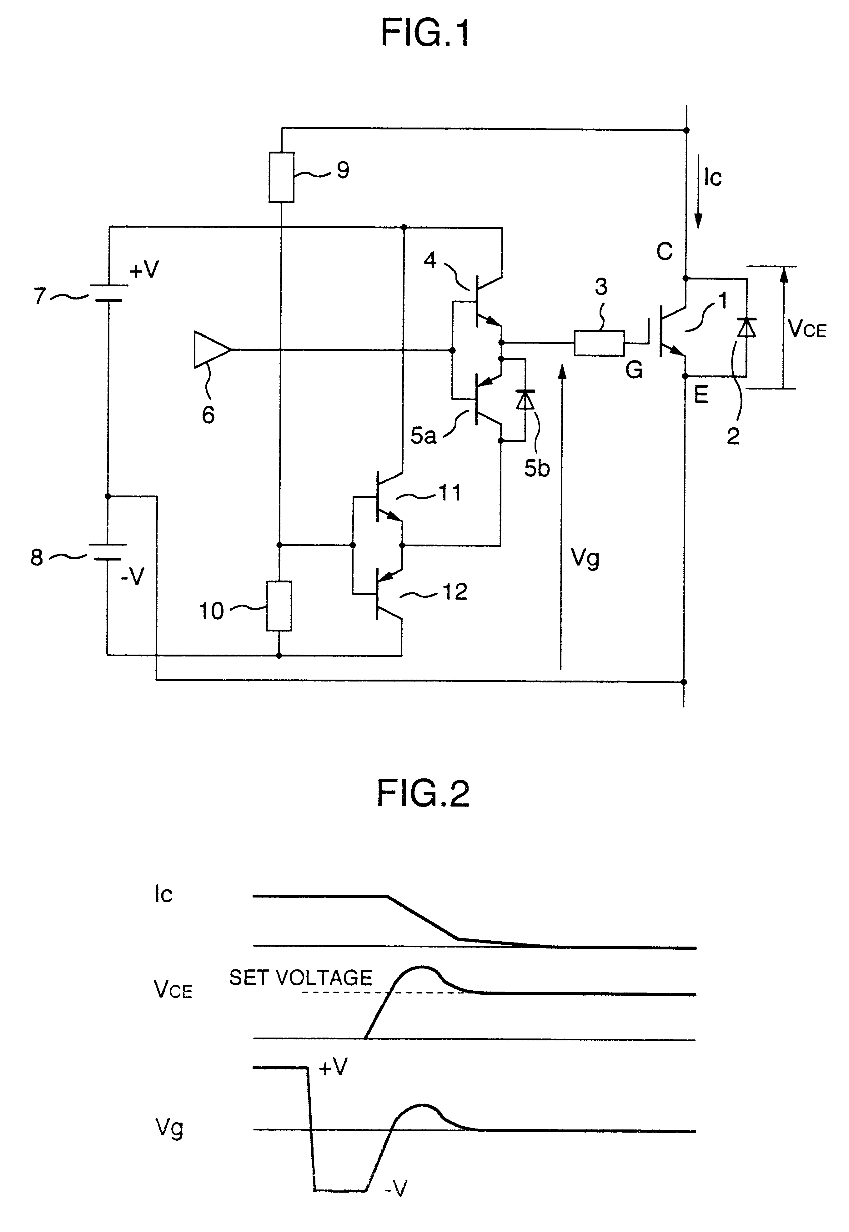
FIG. 1 represents an arrangement of a main circuit in unit of an arm. As indicated in this FIG. 1, in this embodiment mode, a cross-connected diode 2 is connected to an insulated-gate transistor 1, and both a transistor 4 and another transistor 5a are connected to a gate resistor 3. Then, both an ON command and an OFF command are supplied from a control circuit 6 to these transistors 4 and 5a. Also, a power supply 7 and another power supply 8 are provided so as to set bias voltages. As to a collector electrode C of the insulated-gate transistor 1 and a minus-polarity terminal of the power supply 8, a series member constituted by a resistor 9 and a resistor 10 is connected. A voltage appearing between the collector electrode C of the insulated-gate transistor 1 and the minus-polarity terminal of the power supply 8, which is divided by the resistor 9 and the resistor 10, is transferre...

second embodiment

FIG. 4 and FIG. 5 indicate a second embodiment mode of the present invention.

It should be noted that the same reference numerals shown in FIG. 1 will be employed as those for denoting the same, or similar circuit elements used in the second embodiment mode shown in FIG. 4 and FIG. 5, and also other embodiment modes (will be discussed later), and therefore, descriptions thereof are omitted.

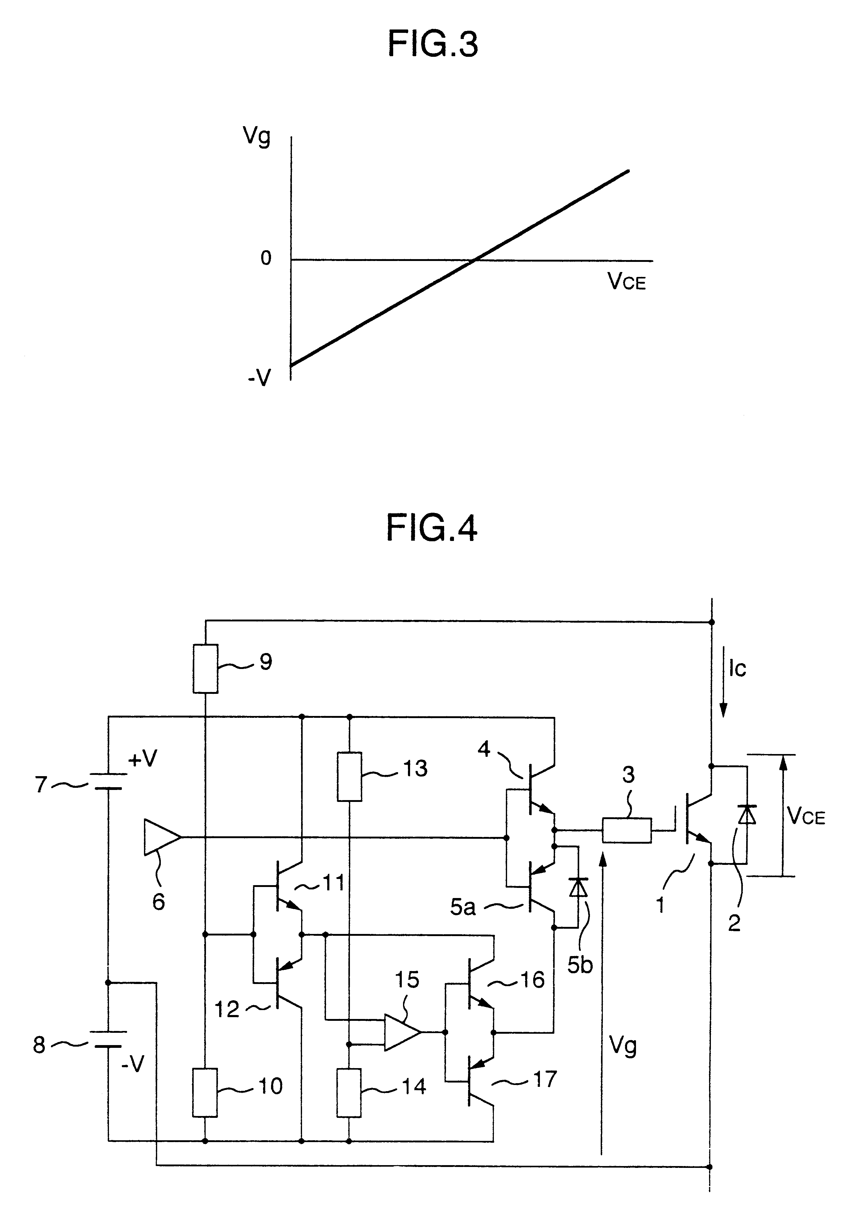
FIG. 4 represents an arrangement of a major circuit in unit of an arm. In this embodiment mode, a voltage detected by a detecting circuit having a similar circuit arrangement to that of the above-explained first embodiment mode is compared with a reference voltage decided by a resistor 13 and a resistor 14 in a comparator 15. The detecting circuit divides a voltage appearing between a collector of an insulated-gate transistor 1 and a minus-polarity terminal of a power supply 8. When a detected voltage is lower than, or equal to the reference voltage, the comparator 15 causes a transistor 16 to be t...

sixth embodiment

FIG. 12, FIG. 13 and FIG. 14 are diagram for indicating a sixth embodiment mode of the present invention.

FIG. 12 represents an arrangement of a main circuit in unit of an arm. Similar to the circuit arrangement of the first embodiment mode, a resistor 10 used to divide a voltage appearing between a collector of an insulated-gate transistor 1 and a minus-polarity terminal of a power supply 8 is subdivided into a resistor 10a and another resistor 10b. A switch 23 is connected in parallel to the resistor 10b. The switch 23 is brought into an OFF state immediately after the insulated-gate transistor 1 is turned OFF, and a V.sub.CE set voltage set by the resistor 9 and the resistors 10a and 10b is brought into a predetermined condition. After a peak voltage by turning OFF the insulated-gate transistor 1 is converged up to the power supply voltage, the switch 23 is turned ON, so that the resistor 10b is shortcircuited. As a result, the set voltage with respect to the voltage V.sub.CE is c...


PUM


Abstract

A semiconductor power converting apparatus includes a semiconductor element for controlling a current flowing between a collector and an emitter in response to a gate condition, a driving device connected to the gate, for driving the gate in response to a drive signal entered thereinto, a voltage applying device for applying both a forward bias and a reverse bias to the gate so as to set the emitter of the semiconductor element to a neutral potential, and a voltage dividing device for dividing a voltage appearing between the collector and the emitter of the semiconductor element, in which the drive signal is under OFF state, a voltage produced based upon the divided voltage by the voltage dividing device is applied to the gate, and the gate voltage is controlled in response to the voltage appearing between the collector and the emitter of the semiconductor element, thereby reducing the snubbed loss.

Description

1. Field of the InventionThe present invention relates to a semiconductor power converting apparatus with employment of a semiconductor element and the like. More specifically, the present invention relates to a semiconductor power converting apparatus capable of suppressing a peak voltage during a switching operation without requiring a snubber circuit.2. Description of the Related ArtIGBTs (Insulated-Gate Bipolar Transistor) known as a typical insulated-gate transistor own low gate power consumption and can be switched in high speeds with a small switching loss. Accordingly, these IGBTs are employed in semiconductor power converting apparatuses having relatively medium and small capacities. Furthermore, these IGBTs are desirably applied to semiconductor power converting apparatuses having large capacities. In general, a jump-up voltage ".DELTA.V" of an IGBT having a snubber circuit is expressed by the following formula (1-1) based upon a capacitance "C" of a snubber capacitor:.DEL...

Claims


Application Information

Patent Timeline
Patent Type & Authority Patents(United States)
IPC IPC(8): H02M1/08H03K17/16H03K4/00H02M1/00
CPCH02M1/08H03K17/168H03K4/00H03K17/166
Inventor SAKAI, HIROMITSUAIZAWA, HIDETOSHIKATOH, SHUJIIYOTANI, RYUJINAGASU, MASAHIRO
Owner HITACHI LTD
Why Eureka
Try Eureka