Semiconductor package and method for fabricating the same

a semiconductor and package technology, applied in the field of semiconductor package, can solve the problems of increased thickness, increased heat, and problematic bga semiconductor package,

Inactive Publication Date: 2002-05-28
AMKOR TECH SINGAPORE HLDG PTE LTD
View PDF124 Cites 340 Cited by
  • Summary
  • Abstract
  • Description
  • Claims
  • Application Information

AI Technical Summary

Benefits of technology

Another object of the invention is to provide a semiconductor package having a structure capable of easily discharging heat from a semiconductor chip included therein, and a method for fabricating the semiconductor package.
Also, the encapsulating process involved in the fabrication of semiconductor packages is conducted in such a fashion that it proceeds from the second major surface of each semiconductor chip in accordance with the present invention. Accordingly, it is possible to achieve a uniform encapsulation while suppressing the occurrence of a wire sweeping phenomenon.

Problems solved by technology

For this reason, an increase in heat occurs inevitably during the operation of such a semiconductor chip.
However, the above mentioned conventional BGA semiconductor package is problematic in that it has an increased thickness because the semiconductor chip is bonded to the upper surface of the circuit board having a relatively large thickness.
As a result, the above mentioned semiconductor package is problematic in that it cannot be applied to a variety of miniature electronic appliances such as portable phones, cellular phones, pagers, and notebooks.
Furthermore, in spite of the increasing heat generated at the semiconductor chip, as mentioned above, there is no appropriate heat discharge means in the conventional semiconductor package.
As a result, the conventional semiconductor package is implicated in a heat-related degradation in the electrical performance and other functions of the semiconductor chip.
In severe cases, the semiconductor package and the electronic appliance using it may be so damaged as not to be inoperable.
Although a semiconductor package has been proposed, which is provided with a heat discharge plate or heat sink for easily discharging heat generated from the semiconductor chip, the provision of such a heat discharge plate causes another problem because it serves to further increase the thickness of the semiconductor package while increasing the manufacturing costs.

Method used


Image

  • Semiconductor package and method for fabricating the same
  • Semiconductor package and method for fabricating the same
  • Semiconductor package and method for fabricating the same

Examples


Embodiment Construction

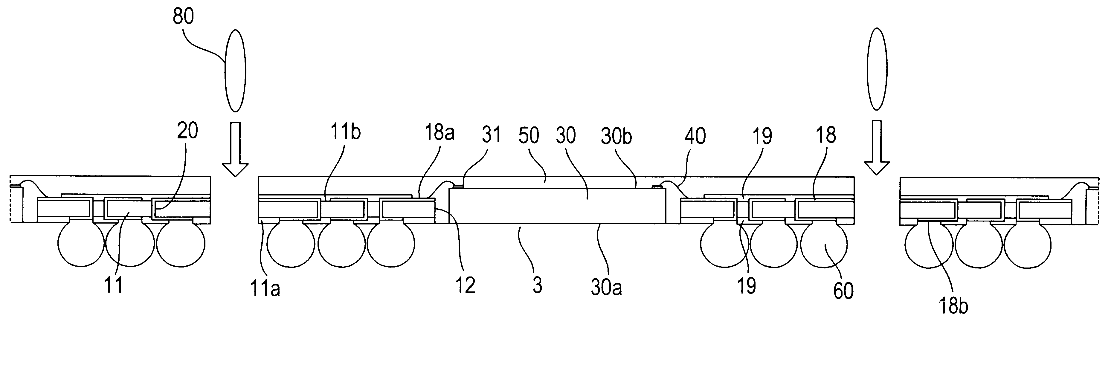
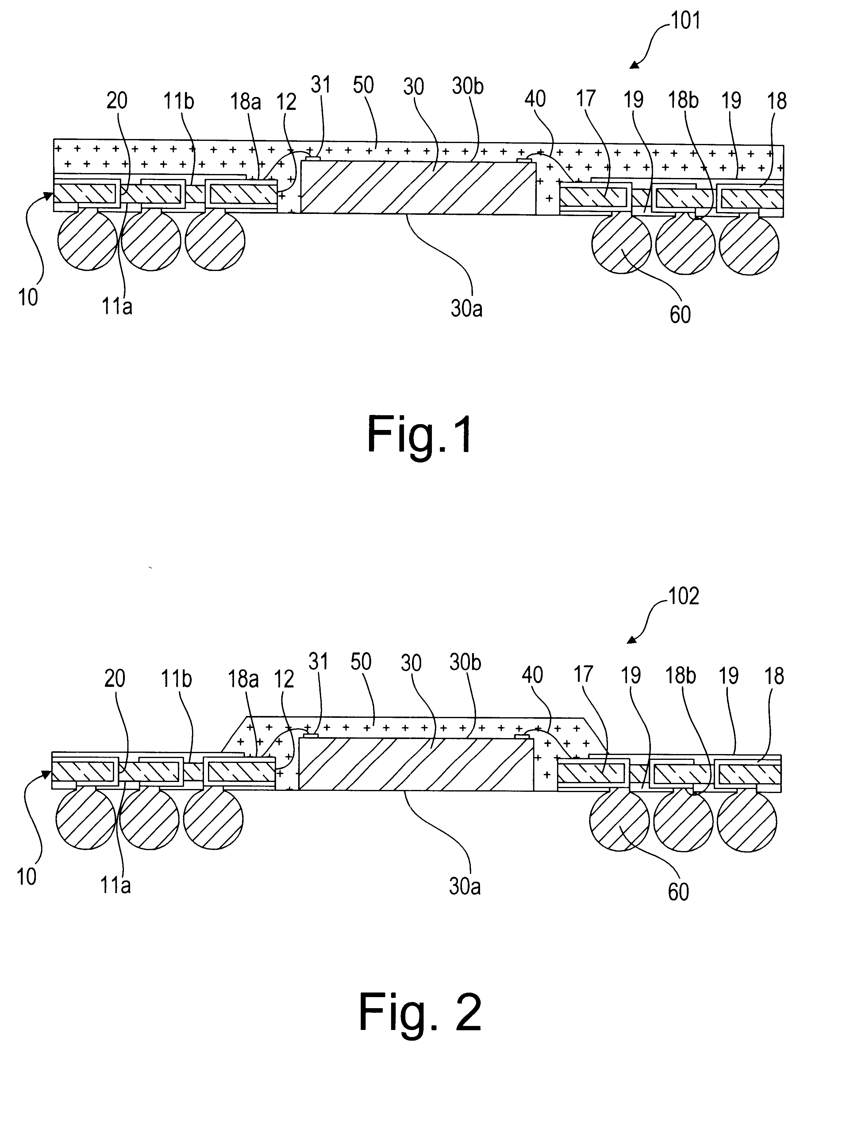
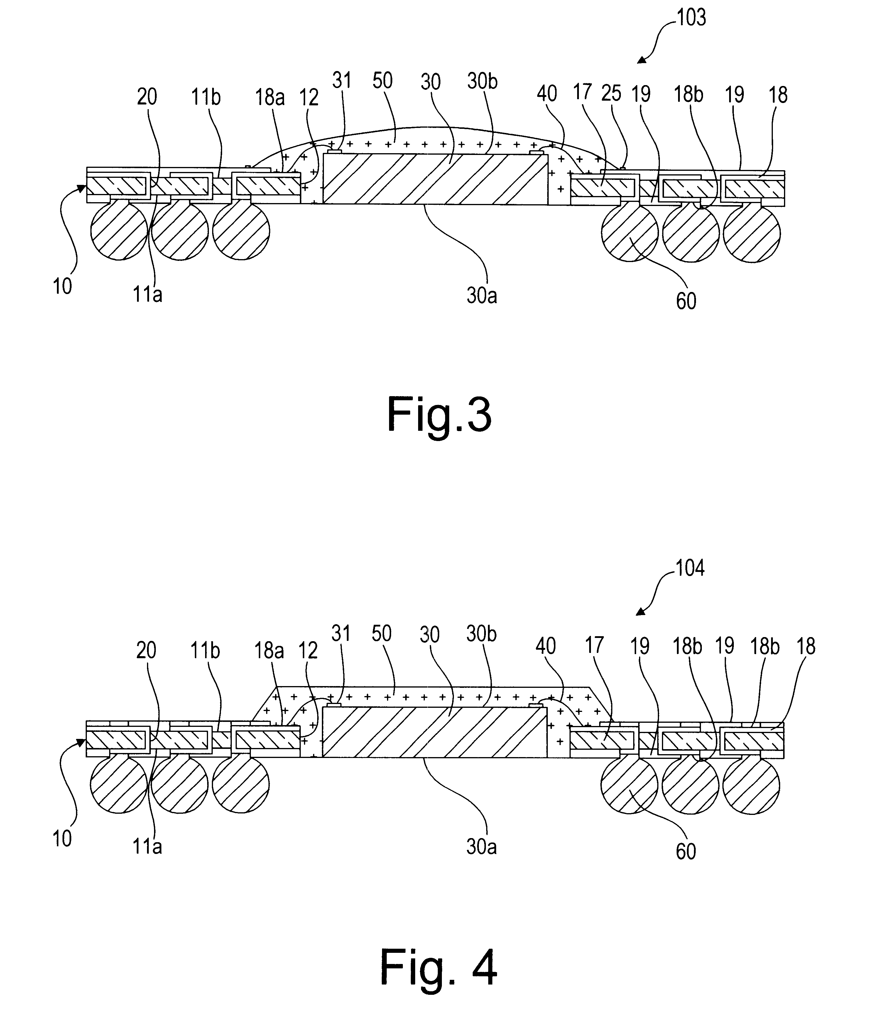
Referring to FIGS. 1 to 5, semiconductor packages according to various embodiments of the present invention are illustrated, respectively.

In accordance with the embodiment of the present invention illustrated in FIG. 1, the semiconductor package, which is denoted by the reference numeral 101, includes a semiconductor chip 30 having a first major surface 30a (a lower surface in FIG. 1) and a second major surface 30b (an upper surface in FIG. 1). A plurality of input / output pads 31 are formed at the second major surface 30b of the semiconductor chip 30.

The semiconductor chip 30 is arranged in such a fashion that it is received in a through hole 12 formed 10 through a circuit board 10 to have a desired size. The through hole 12 has a size larger than the area of the first or second surface 30a or 30b of the semiconductor chip 30. The circuit board 10 includes a resin substrate 17 having a first major surface 11a (a lower surface in FIG. 1) and a second major surface 11b (an upper surfa...


PUM


Abstract

Semiconductor packages having a thin structure capable of easily discharging heat from a semiconductor chip included therein, and methods for fabricating such semiconductor packages, are disclosed. An embodiment of a semiconductor package includes a semiconductor chip having a first major surface and a second major surface, the semiconductor chip being provided at the second major surface with a plurality of input / output pads; a circuit board including a resin substrate having a first major surface and a second major surface, a first circuit pattern formed at the first major surface and provided with a plurality of ball lands, a second circuit pattern formed at the second major surface and provided with a plurality of bond fingers connected with he ball lands by conductive via holes through the resin substrate, cover coats respectively coating the first and second circuit patterns while allowing the bond fingers and the ball lands to be exposed therethrough, and a central through hole adapted to receive the semiconductor chip therein; electrical conductors that electrically connect the input / output pads of the semiconductor chip with the bond fingers of the circuit board, respectively; a resin encapsulate that covers the semiconductor chip, the electrical conductors, and at least part of the circuit board; and, a plurality of conductive balls fused on the ball lands of the circuit board, respectively.

Description

I. Field of the InventionThe present invention relates to a semiconductor package and a method for fabricating the semiconductor package.II. Description of the Prior ArtRecently, semiconductor devices have been developed to have a thinner and more miniature structure. For such semiconductor devices, there are ball grid array (BGA) semiconductor packages, chip scale semiconductor packages, and micro BGA semiconductor packages.Also, semiconductor chips, which are mounted on semiconductor packages as mentioned above, have been developed toward a high performance of electric power circuits, an increase in operating frequency, and an expansion of circuit functions, in pace with the development of integration techniques and manufacturing equipment. For this reason, an increase in heat occurs inevitably during the operation of such a semiconductor chip.Referring to FIG. 10, a typical BGA semiconductor package having a conventional structure involving the above mentioned problem is illustra...

Claims


Application Information

Patent Timeline
Patent Type & Authority Patents(United States)
IPC IPC(8): H01L21/68H01L21/02H01L23/12H01L23/48H01L23/31H01L23/28H01L21/56H01L21/67H01L23/498H01L23/544H01L25/10H01L23/13
CPCH01L21/56H01L21/565H01L21/568H01L23/13H01L23/3128H01L23/49816H01L23/49838H01L23/544H01L24/96H01L24/97H01L25/105H01L21/561H01L2924/01028H01L24/45H01L2223/54473H01L2224/45124H01L2224/45144H01L2224/48091H01L2224/48227H01L2224/81005H01L2224/85001H01L2224/97H01L2924/01002H01L2924/01004H01L2924/01013H01L2924/01029H01L2924/01046H01L2924/01047H01L2924/0105H01L2924/01079H01L2924/01082H01L2924/15151H01L2924/15311H01L2924/15331H01L2924/18165H01L2225/1058H01L2225/1035H01L2924/01033H01L24/48H01L2924/00014H01L2224/85H01L2924/181H01L2924/00012
Inventor SHIN, WONSUNCHUN, DOSUNGLEE, SANGHOLEE, SEONGOODICAPRIO, VINCENT
Owner AMKOR TECH SINGAPORE HLDG PTE LTD
Why Eureka
Try Eureka