Hermatic firewall for MEMS packaging in flip-chip bonded geometry

a technology of flip-chip and geometry, applied in the field of microelectromechanical system (mems) packaging, can solve the problems of expensive process for packaging mems devices in such systems, incompatible with mems device operation, and expensive ceramic packaging usually chosen over cos

Inactive Publication Date: 2002-06-04
LUCENT TECH INC
View PDF9 Cites 82 Cited by
  • Summary
  • Abstract
  • Description
  • Claims
  • Application Information

AI Technical Summary

Problems solved by technology

Packaging MEMS devices in such systems is in general a costly process.
However, these packaging techniques usually involve treatment of semiconductor chips using a fluid, and are therefore not compatible with MEMS device operation.
For this reason, expensive ceramic packaging has usually been chosen over cost-effective plastic molded packages for MEMS devices.
Packaging MEMS devices cost-effectively under these conditi

Method used


Image

  • Hermatic firewall for MEMS packaging in flip-chip bonded geometry
  • Hermatic firewall for MEMS packaging in flip-chip bonded geometry
  • Hermatic firewall for MEMS packaging in flip-chip bonded geometry

Examples


Embodiment Construction

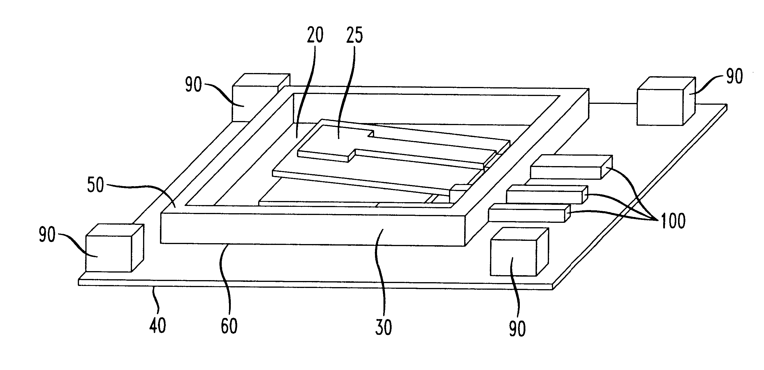
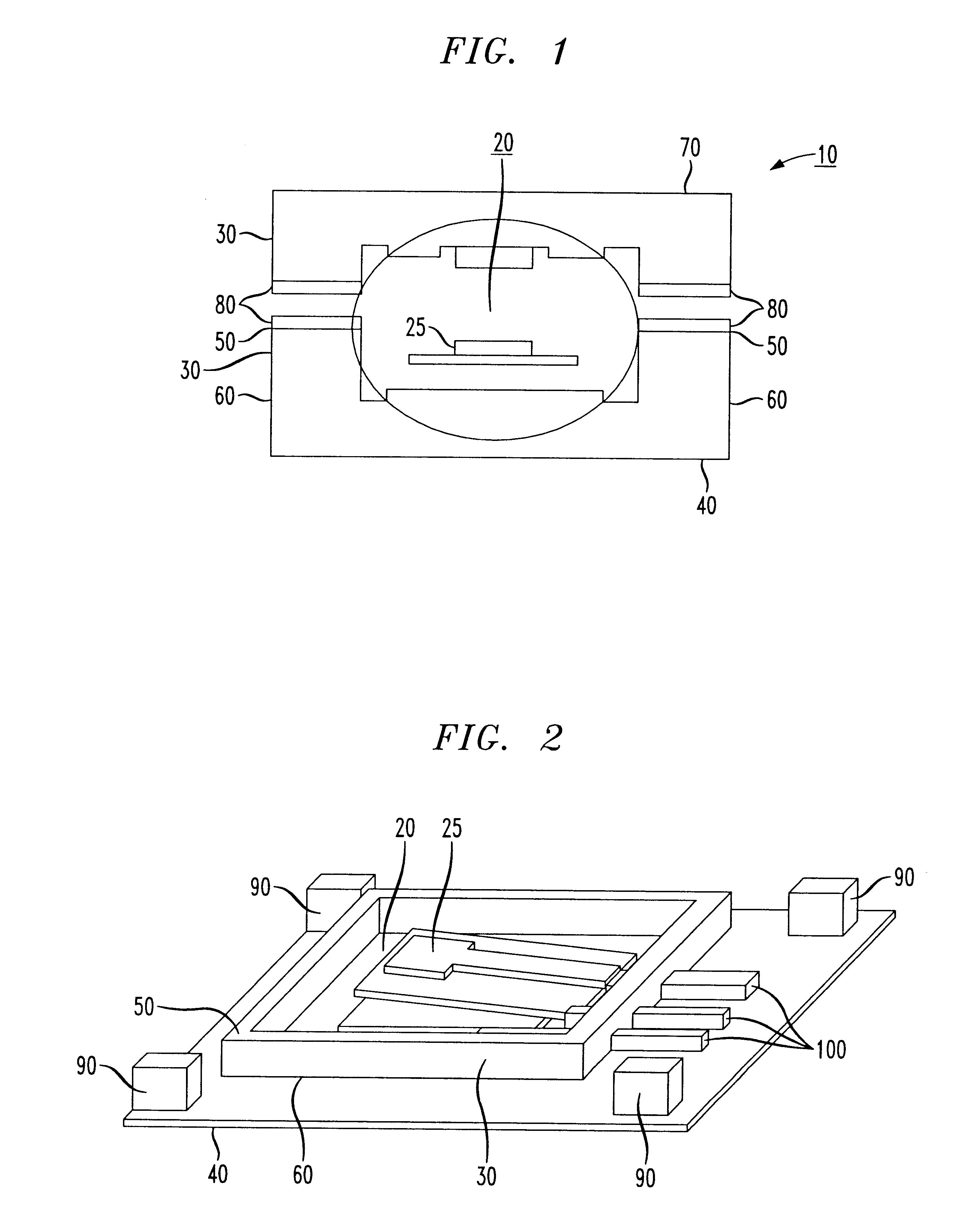
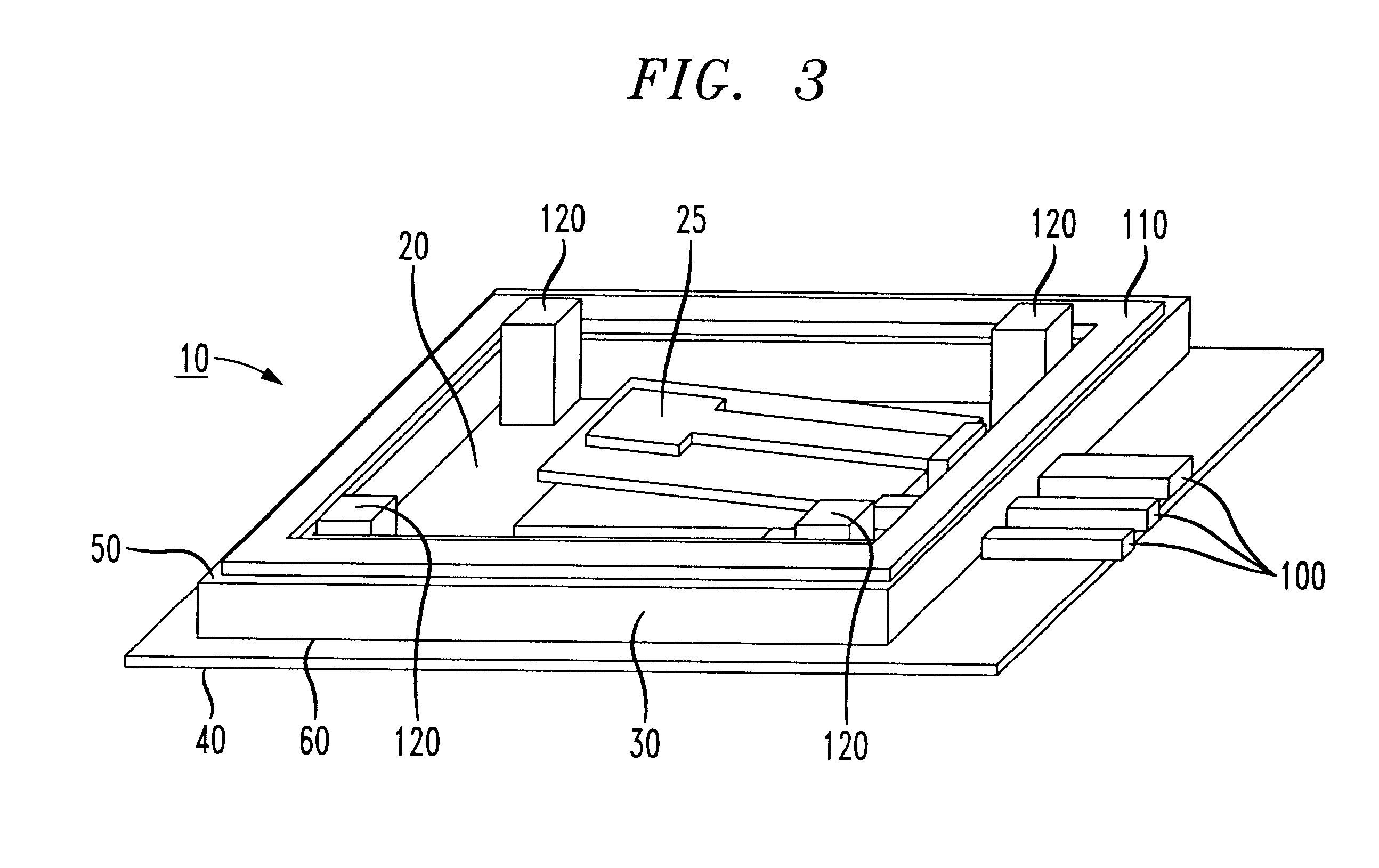
Referring now to the drawings, FIG. 1 depicts a schematic cross-sectional view of the hermetic firewall structure of the present invention identified by the general reference numeral 10. The package 10 comprises a cavity 20 for enclosing a MEMS device 25 or several MEMS devices, depending on the particular hybrid circuit application in which the MEMS device(s) will be integrated. In a preferred embodiment, a firewall 30 is fabricated on one or both substrates 40 and 70 on one of which the MEMS device is fabricated. The firewall 30 includes a top surface 50 and a bottom surface 60. The package 10 further comprises a second substrate 70 which is bonded to the first substrate through the firewall 30 formed on substrate 40. The second substrate 70 contains a mating seal to the firewall 30, which completes the firewall structure. Preferably, the second substrate is "flip-chip" bonded to substrate 40, using a suitable bonding technique. A preferred bonding technique is a heat-based proces...


PUM


Abstract

A package for hermetically sealing a micro-electromechanical systems (MEMS) device in a hybrid circuit comprise a firewall formed on a substrate for the MEMS device and which has a height defining a cavity of the package in which the MEMS device will be sealed. A second substrate spaced from the first substrate hermetically seals the cavity when the second substrate is flip-chip bonded to the first substrate and soldered to the first substrate with a thin film metal material placed on at least a top portion of the firewall. The resulting firewall MEMS device package can be further packaged using conventional CMOS packaging techniques. By hermetically sealing the cavity, the enclosed MEMS device is protected from deleterious conditions found in the environment of conventional CMOS packaging techniques which is often detrimental to MEMS device function.

Description

1. Field of the InventionThe present invention relates to packaging for micro-electromechanical systems (MEMS) devices. More specifically, the present invention relates to packaging of MEMS devices in flip-chip bonded geometry to provide hermetic seals for the MEMS devices.2. Description of the Related ArtMEMS devices have become ubiquitous in the semiconductor industry and are used in hybrid electrical and mechanical functions that are necessary in many electronic and electro-optical systems. Packaging MEMS devices in such systems is in general a costly process. Because mechanical motion is an essential part of the MEMS function, a carefully designed space for the motion is needed in order for the MEMS device to operate reliably. Conventional packaging techniques used for CMOS electronics are performed after the CMOS devices are appropriately protected using proper passivation material. Such passivation procedure protects the devices from the packaging processes that are usually me...

Claims


Application Information

Patent Timeline
IPC IPC(8): B81B7/00H01L23/10H01L23/057H01L23/04H01L23/02B81B1/00
CPCB81B7/0041H01L23/04H01L23/057H01L23/10B81C2203/019H01L2924/0002H01L2924/01079H01L2924/00
Inventor BISHOP, DAVID JOHNGATES, II, JOHN VANATTAKIM, JUNGSANG
Owner LUCENT TECH INC
Why Eureka
Try Eureka