Chain-connected shift register and programmable logic circuit whose logic function is changeable in real time
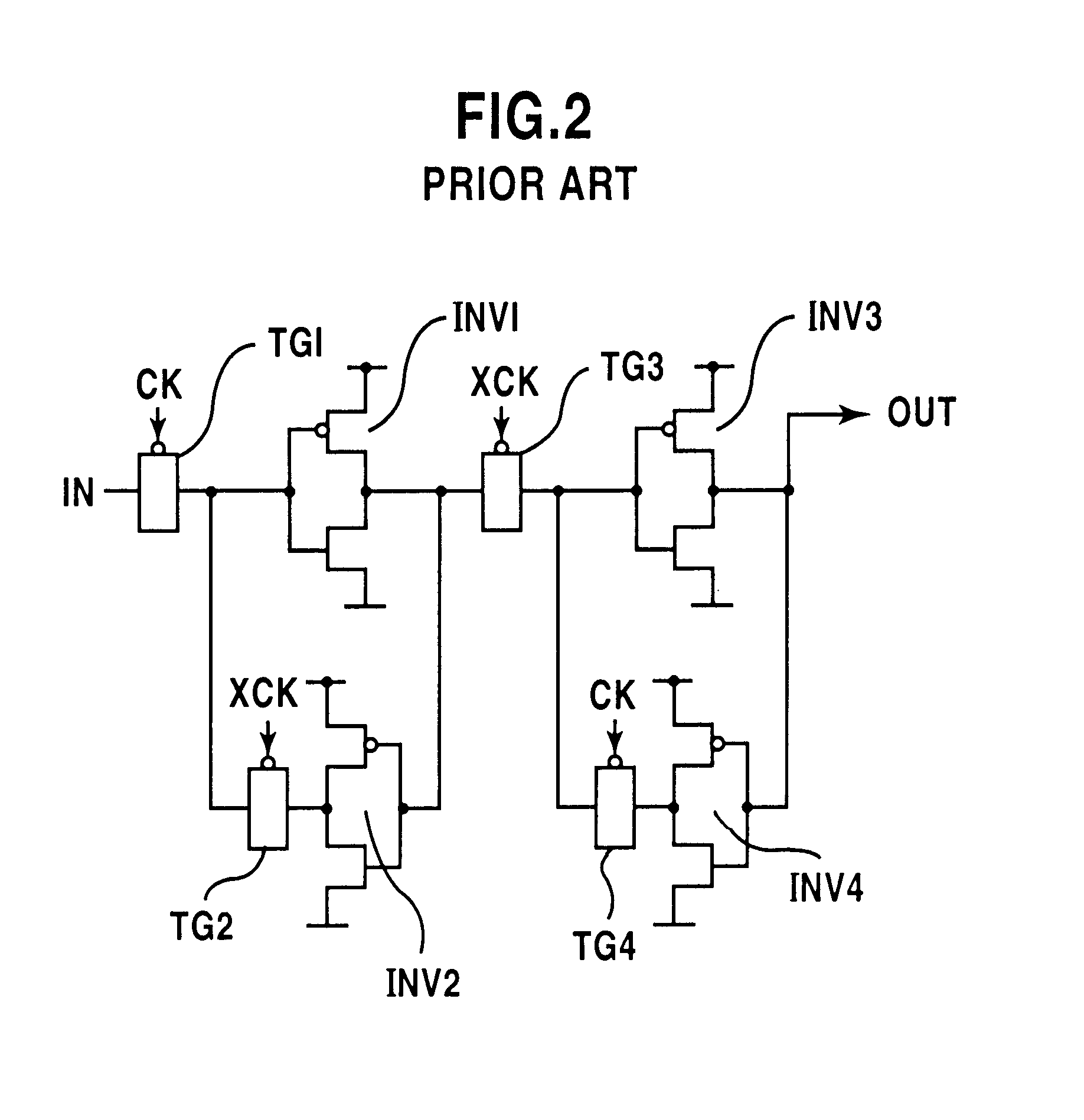
a technology of a shift register and a logic function, which is applied in the field of chain-connected shift register and a programmable logic circuit, can solve the problems of difficult to obtain a stable operation in the shift register of the prior-art shift register constructed with such d-type flip-flops, requiring a relatively large area on the lsi chip, and requiring a large area
- Summary
- Abstract
- Description
- Claims
- Application Information
AI Technical Summary
Problems solved by technology
Method used
Image
Examples
second embodiment
FIG. 19 shows another modification of the shift register according to the present invention shown in FIG. 16. In the shift register shown in FIG. 19, for the switches, the transmission gates and the P-channel MOS transistors are used, and instead of the inverters, NOR gates are used. Also, in the circuit cells b, c, instead of the clock supplying circuit shown in FIG. 6, the clock distributor shown in FIG. 17 is provided.
The clock distributor is provided with the clock signals CK, XCK for the shift register, the clock signals DCK, XDCK for the D-type flip-flop, and the control signals PGM, MODE for selecting one of the two operation modes (shift register and D-type flip-flop modes).
In the shift register shown in FIG. 19, by supplying the given signals to input terminals R, S of the NOR gates, a state of a portion of the shift register may be set to be a desired state. Further, a state of the formed flip-flop may be also set to be a desired state.
Next, a description will be given of ...
first embodiment
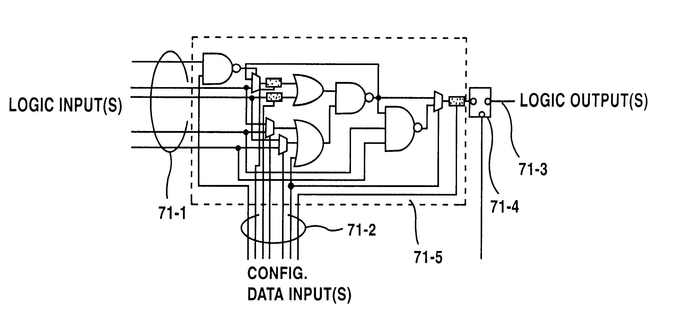
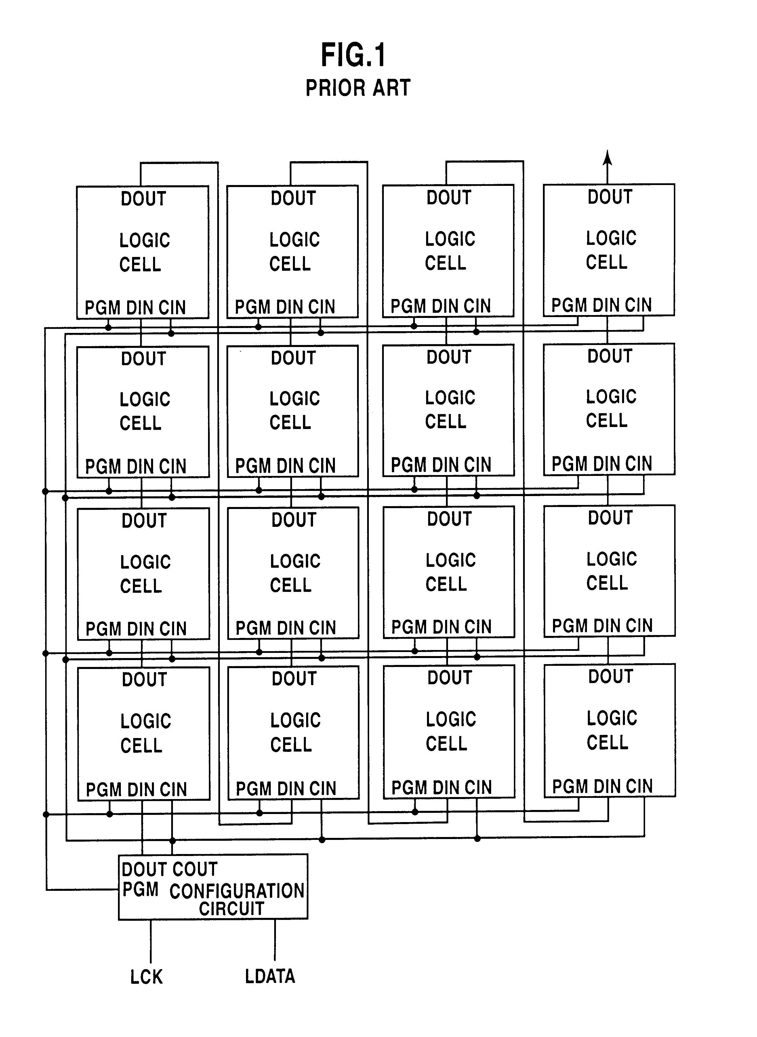
FIG. 20 shows a block diagram of a programmable logic circuit according to the present invention. A logic cell in the programmable logic circuit includes a programmable function unit and a configuration memory for determining a function of the programmable function unit. The programmable. function unit may include several flip-flops. The configuration memory is constructed with the shift register shown in FIG. 16. The shift register has circuit cells M0, M1, MFF, M2, M3. The circuit cells M0, M1, M2, M3 respectively have the same circuit configuration as that of the above-discussed circuit cell a. The circuit cell MFF has substantially the same circuit configuration as that of the circuit cell b, c shown in FIG. 16. Therefore, the circuit cell MFF is operable as a flip-flop.
A clock distributor CKD shown in FIG. 20 has substantially the same configuration as that of the clock distributor shown in FIG. 16. The clock distributor CKD is provided with the clocks CK, XCK for the shift reg...
PUM
 Abstract
Description
Claims
Application Information


