Excess delay compensation in a delta sigma modulator analog-to-digital converter

a delta sigma modulator and analog-to-digital converter technology, applied in digital-analog converters, transmission systems, instruments, etc., can solve the problems of granular noise, distortion, and quantization noise in the output digital signal, and achieve the effect of reducing the noise of overload

Inactive Publication Date: 2002-07-02
RAYTHEON CO
View PDF5 Cites 74 Cited by
  • Summary
  • Abstract
  • Description
  • Claims
  • Application Information

AI Technical Summary

Problems solved by technology

Quantization error results in quantization noise in the output digital signal, which is also called granular noise.
When an analog sample is too large to be accurately digitally represented by to the quantizer (given the fixed number of quantizer bits), clipping occurs, resulting in distortion called overload noise.
Unfortunately, adding additional resolution required to obtain sufficient SNR's is often costly.
Unfortunately, typical oversampling ADC's are still particularly susceptible to overload distortion and granular noise.
Unfortunately, conventional .DELTA..SIGMA.
ADC's are often difficult to implement and are susceptible to noise resulting from delays in the quantizer feedback path.
The delays include signal dependent jitter delay, latch delay, and DAC cell switching delays.
However, the additional RZ DAC's are often expensive and difficult to implement accurately.
ADC's, the RZ DAC's in the quantizer feedback path may have insufficient time to settle to zero, resulting in poor ADC performance.
However, this approach still fails to effectively compensate for signal dependent jitter and other delays.
Finite DAC cell switching delays in the multi-bit feedback DAC's are also problematic.
As is known in the art, multi-bit DAC's have hardware limitations that result in glitches in signal output by circuits employing these devices.
Glitches result when less than all of the bits in a DAC change simultaneously.
The glitches cause spurious frequency tones, i.e., glitch noise, to appear at the DAC output very close to the desired output frequency.
ADC and adversely affect circuit stability, especially in fourth order or higher order .DELTA..SIGMA.
DAC's with excellent amplitude resolution and frequency response tend to consume excess power and are expensive.
In addition, spurious tones become more problematic as the frequency of the periodic signal increases.
This further limits the range of allowable output frequencies.
Consequently, the quantizer comparators switch and regenerate at different times, which results in undesirable signal dependent jitter delay.
ADC's employing RZ DAC's often fail to address signal dependent jitter.
Signal dependent jitter is an additional source of loop delay in the quantizer feedback path.
The additional loop delay reduces the dynamic performance of the ADC and may reduce feedback loop stability.
The feedback delays include signal dependent jitter delay and feedback digital-to-analog converter cell switching delays.

Method used


Image

  • Excess delay compensation in a delta sigma modulator analog-to-digital converter
  • Excess delay compensation in a delta sigma modulator analog-to-digital converter
  • Excess delay compensation in a delta sigma modulator analog-to-digital converter

Examples


Embodiment Construction

While the present invention is described herein with reference to illustrative embodiments for particular applications, it should be understood that the invention is not limited thereto. Those having ordinary skill in the art and access to the teachings provided herein will recognize additional modifications, applications, and embodiments within the scope thereof and additional fields in which the present invention would be of significant utility.

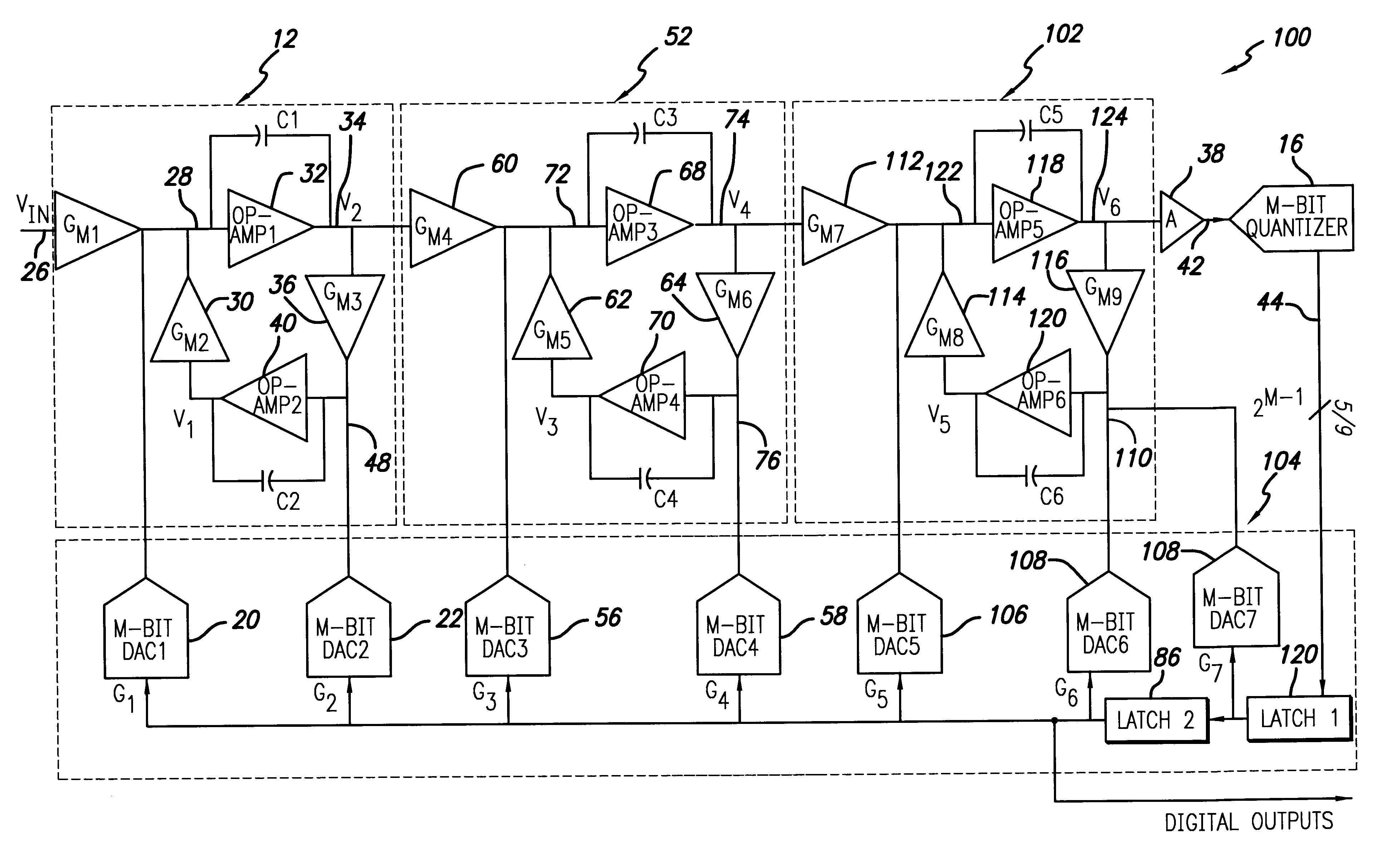
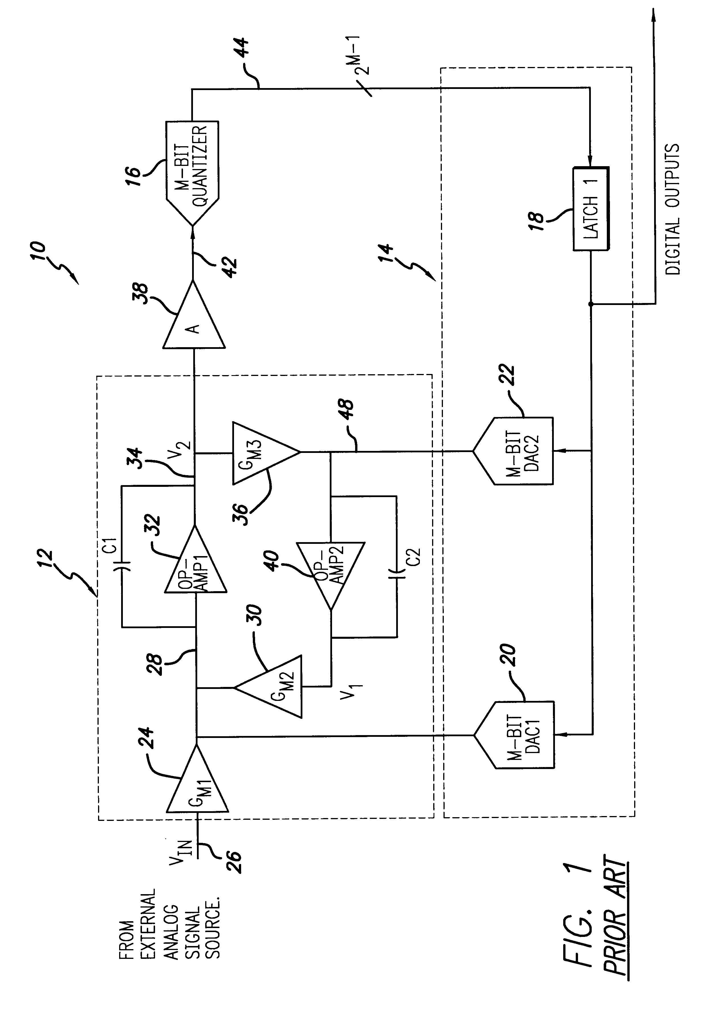
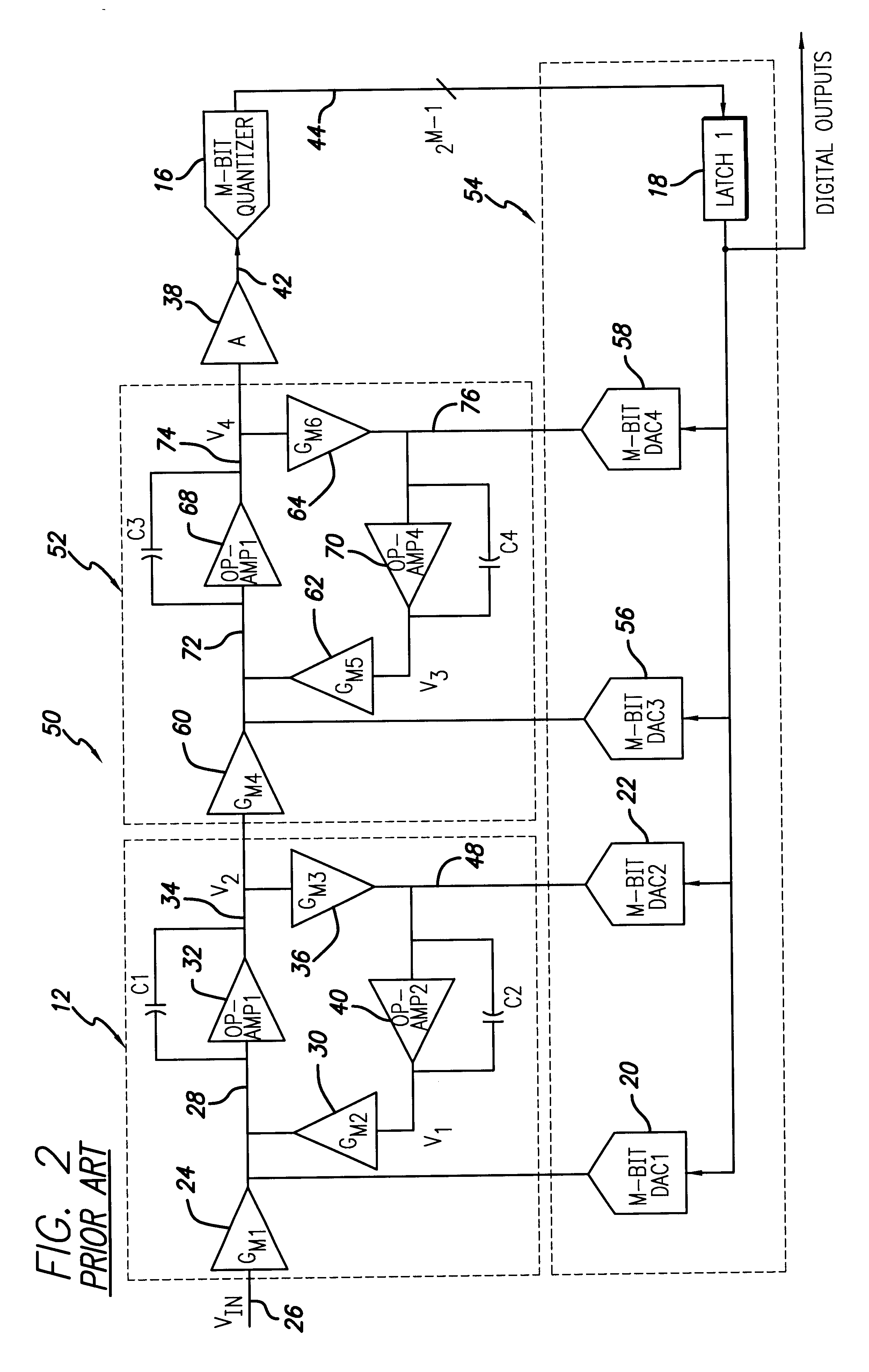
FIG. 1 is a diagram of a conventional second order .DELTA..SIGMA. ADC 10. The .DELTA..SIGMA. ADC includes a resonator stage 12 (bandpass loop filter) and an m-bit quantizer feedback-DAC path 14 from the output of an m-bit quantizer 16 back to the resonator stage 12. The feedback path 14 includes a first latch 18, which is connected at an output of the m-bit quantizer 16. An output of the first latch 18 is connected to an input of a first m-bit digital-to-analog converter (DAC) 20 and to an input of a second DAC 22.

The resonator stage 12 inc...


PUM


Abstract

A high-performance delta sigma analog-to-digital converter. The high-performance delta sigma analog-to-digital converter includes a first mechanism for converting an input analog signal to a digital output signal. The first mechanism is characterized by a transfer function that is altered relative to an ideal transfer function. A second mechanism compensates for the alteration in the transfer function via a single additional digital-to-analog converter. In a specific embodiment, the alteration includes an additional pole and an additional zero induced by feedback delays in the first mechanism. The feedback delays include signal dependent jitter delay and feedback digital-to-analog converter cell switching delays. The second mechanism includes an additional latch that compensates for the signal dependent jitter delay. The first mechanism includes a resonator and a quantizer. The second mechanism includes a feedback path from an output of the quantizer to the resonator. The feedback path includes a first latch positioned between an output of the quantizer and the additional digital-to-analog converter. The additional latch is positioned at an output of the first latch and eliminates signal dependent jitter delay in the analog-to-digital converter. The additional feedback digital-to-analog converter is a non-return-to-zero digital-to-analog converter, an output of which is connected to the resonator.

Description

1. Field of InventionThis invention relates to analog-to-digital converters. Specifically, the present invention relates to high-performance delta sigma analog-to-digital converters.2. Description of the Related ArtAnalog-to-digital converters (ADC's) are employed in a variety of demanding applications including computer modems, wireless telephones, and satellite receiver systems. Such applications demand cost-effective ADC's that can efficiently convert an analog input signal to digital output signal over a wide range of frequencies and signal magnitudes with minimal noise and distortion.An ADC typically converts an analog signal to a digital signal by sampling the analog signal at predetermined sampling intervals and generating a sequence of binary numbers via a quantizer in response thereto. The sequence of binary numbers is a digital signal representation of the sampled analog signal.The length of a binary number assigned to a given sampled value of the analog signal corresponds...

Claims


Application Information

Patent Timeline
Patent Type & Authority Patents(United States)
IPC IPC(8): H03M3/04H03M3/00H03M3/02
CPCH03M3/37H03M3/406H03M3/424H03M3/454
Inventor CHENG, WILLIAM W.
Owner RAYTHEON CO
Why Eureka
Try Eureka