Method and apparatus for selecting functional space in a low pin count memory device

a memory device and low pin count technology, applied in the field of memory in processor-based or microcontroller-based systems, can solve the problem of particular problem of dedicated pin for accessing one of several functional spaces

Inactive Publication Date: 2002-07-16
INTEL CORP
View PDF6 Cites 23 Cited by
  • Summary
  • Abstract
  • Description
  • Claims
  • Application Information

AI Technical Summary

Problems solved by technology

This mapping scheme presents several problems, the most significant of which is the resulting error created when an access to the main memory is mapped to that intended for the register space.
The implementation of a dedicated pin for accessing one of several functional spaces is particularly problematic in Low Pin Count (LPC) (refer to http: / / developer.intel.com / design / chipsets / industry / lpc.sub.-- 100.pdf) memory devices, as a minimal number of pins are implemented in these devices so as to reduce the requirements for space, cost and testing procedures.

Method used


Image

  • Method and apparatus for selecting functional space in a low pin count memory device
  • Method and apparatus for selecting functional space in a low pin count memory device
  • Method and apparatus for selecting functional space in a low pin count memory device

Examples


Embodiment Construction

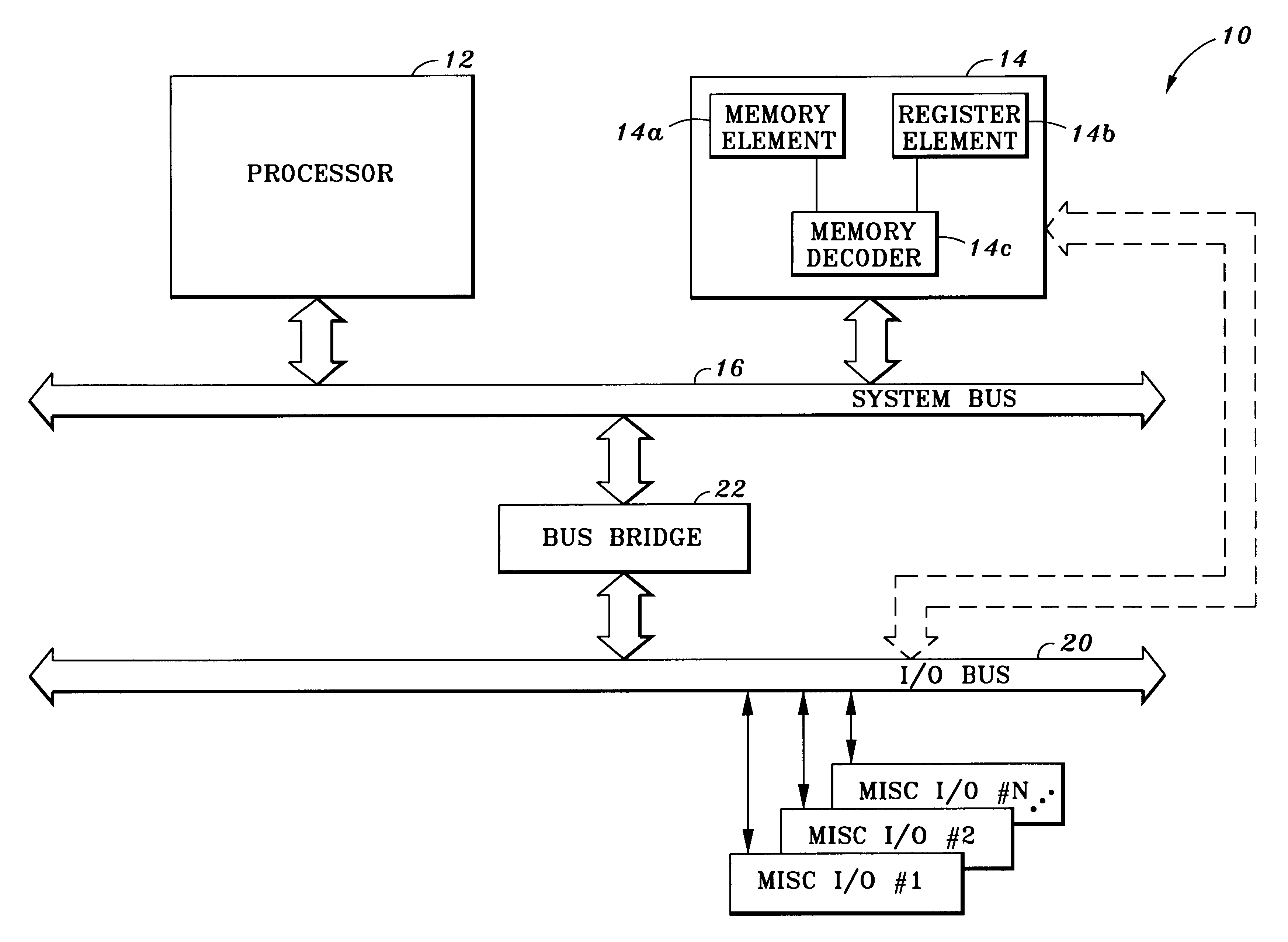
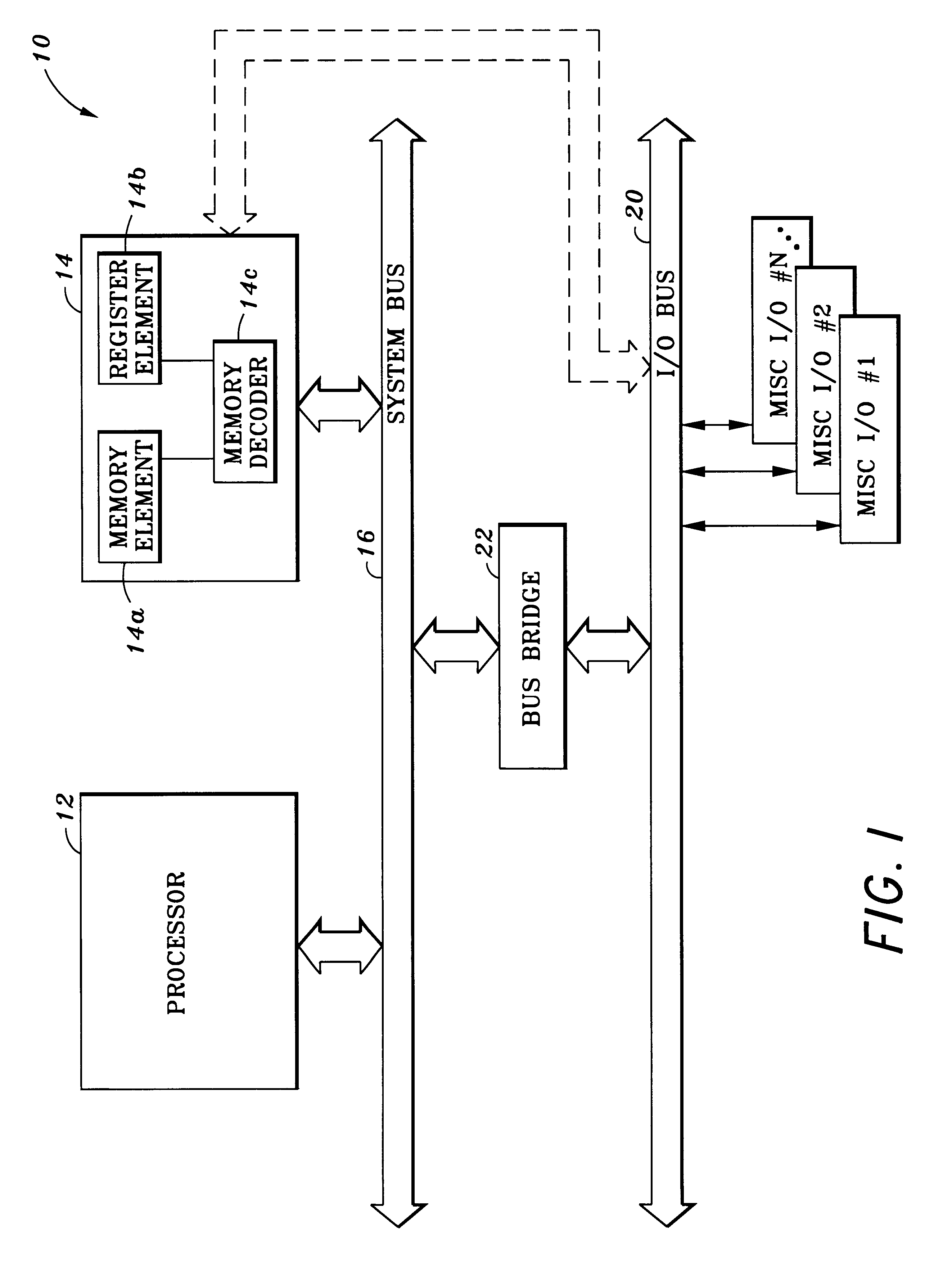
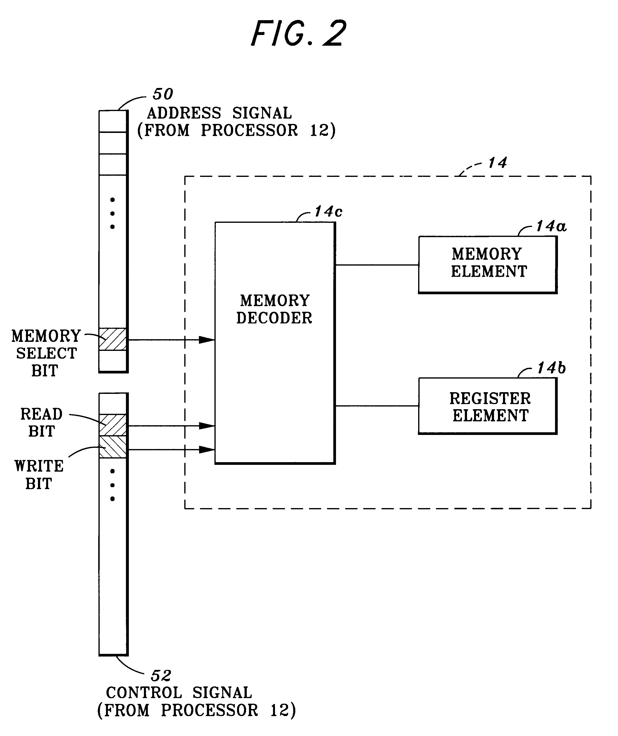
The present invention utilizes a memory configuration bit located in an address to indicate the use of either of the memory space or the register space in a low pin count (LPC) memory device, for the associated operation. In one embodiment, the memory select bit is located adjacent the most significant address bit in the address.

The present embodiment is described in reference to a processor system 10. FIG. 1 illustrates an exemplary LPC processor system 10 which implements the processes of the present invention. The processor system 10 comprises a processor 12 (such as a central processing unit) and a memory module 14. The memory module 14 includes a standard memory location 14a, a register location 14b and a memory decoder 14c. In one embodiment, the memory module 14 is a main memory that may be implemented by a random access memory (RAM) or a flash memory or a combination thereof. The processor 12 and memory module 14 are coupled to a system bus 16. In one alternate embodiment, t...


PUM


Abstract

The present invention is an apparatus and method for selecting one of a first and a second storage element in response to a control signal issued by a processor in a low pin count device. The apparatus comprises a decoder to receive the control signal and an address signal having a select bit indicative of one of the first and the second storage elements. The decoder generates a select signal to access one of the first and the second storage elements based on the select bit.

Description

1. Field of the InventionThe present invention relates generally to memory in processor-based or microcontroller-based systems, and more particularly, to an apparatus and method of selecting functional space in a low pin count memory device.2. Description of the Related ArtIn processor-based systems such as computers, an address space may correspond to several functional spaces. To allow the processor to access these functional spaces, extra signals or signal lines are used. For example, a dedicated pin is typically provided on a chip so as to access a separate functional space in a memory component, such as register space. Such a separate functional space in the memory component is typically mapped to the same address space as the main memory, i.e., to memory space. This mapping scheme presents several problems, the most significant of which is the resulting error created when an access to the main memory is mapped to that intended for the register space. The implementation of a de...

Claims


Application Information

Patent Timeline
Patent Type & Authority Patents(United States)
IPC IPC(8): G06F12/06
CPCG06F12/06
Inventor POISNER, DAVID I.
Owner INTEL CORP
Why Eureka
Try Eureka