Auto correction of error checked simulated printed images

a printing image and error correction technology, applied in the field of integrated circuit layout modeling, can solve the problems of diffraction effects introducing the need for additional complex design rules, conventional approaches do not account for photolithographic or other process effects on the net process window, and deviations between

Inactive Publication Date: 2002-07-23
IBM CORP
View PDF12 Cites 235 Cited by
  • Summary
  • Abstract
  • Description
  • Claims
  • Application Information

AI Technical Summary

Problems solved by technology

However, such conventional approaches do not account for photolithographic or other process effects on the net process window.
As the minimum feature size in semiconductor integrated circuit technology is pushed below the wavelength of the light used to transfer the mask images to the wafers, diffraction effects introduce the need for additional complex design rules.
In addition, other physical effects such as localized etch variations, mask distortions, lens distortions, and topography related effects introduce deviations between the desired and actual printed patterns on the wafer.
These complexities make it difficult both to do the design layout and the design rule checking (DRC) correctly.
Conventional systems utilize very complicated rule sets, have an approach limited to nominal processing quality, and do not account for real world manufacturing complications.
Further, the altering may add notches to the working design data set.

Method used


Image

  • Auto correction of error checked simulated printed images
  • Auto correction of error checked simulated printed images
  • Auto correction of error checked simulated printed images

Examples


Embodiment Construction

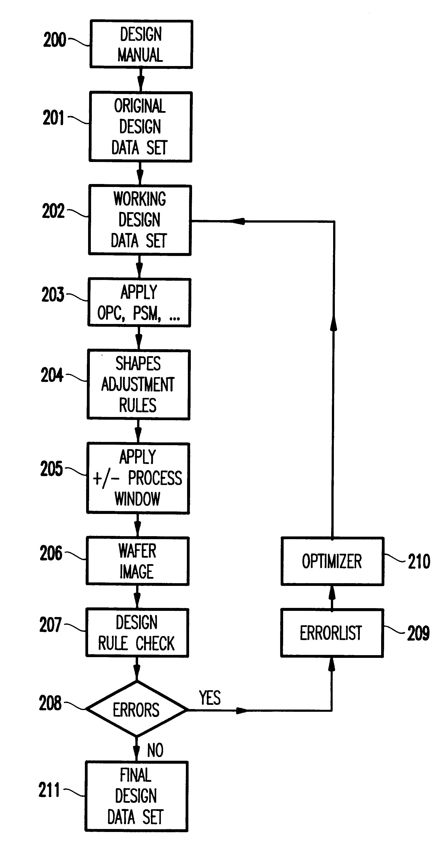
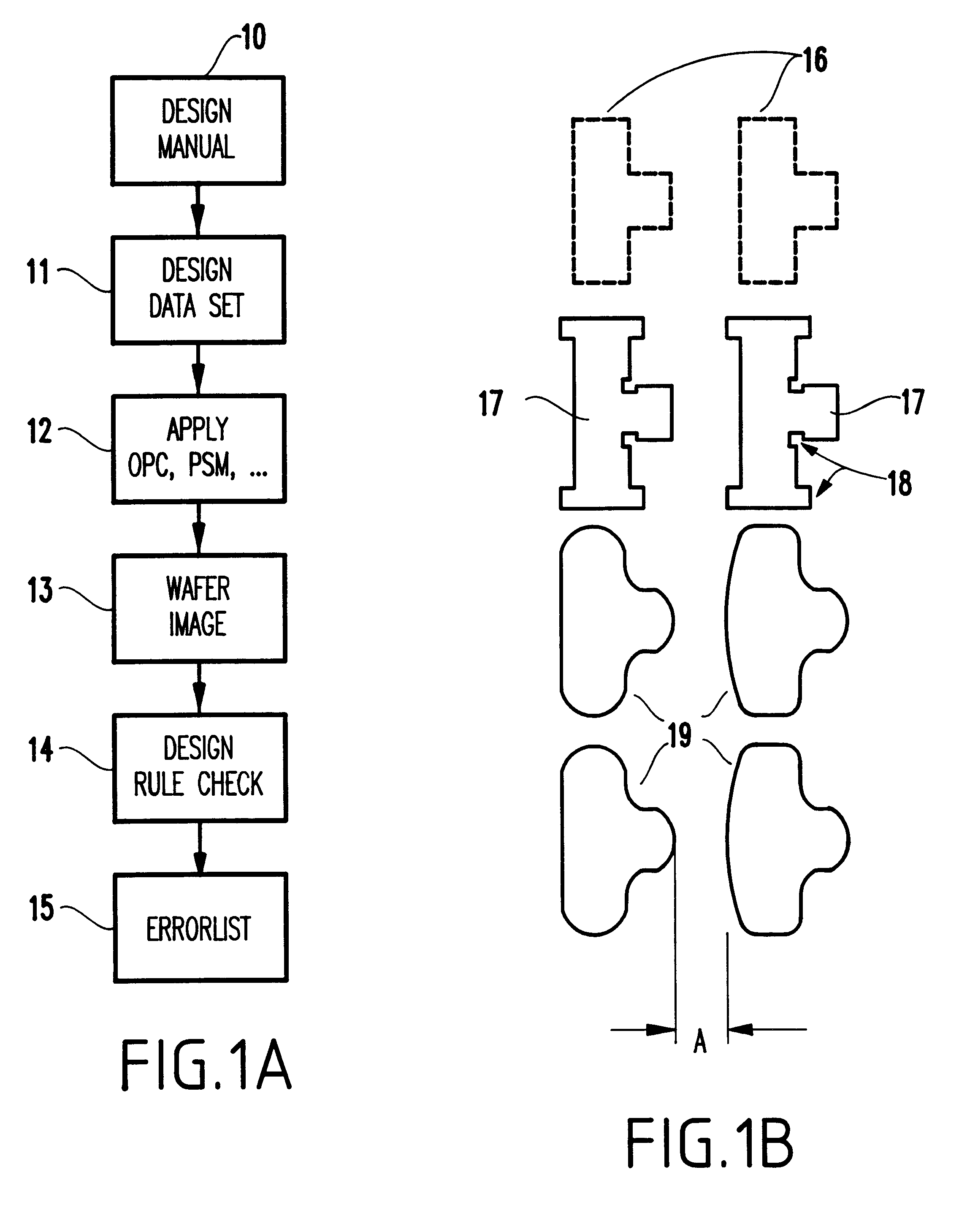
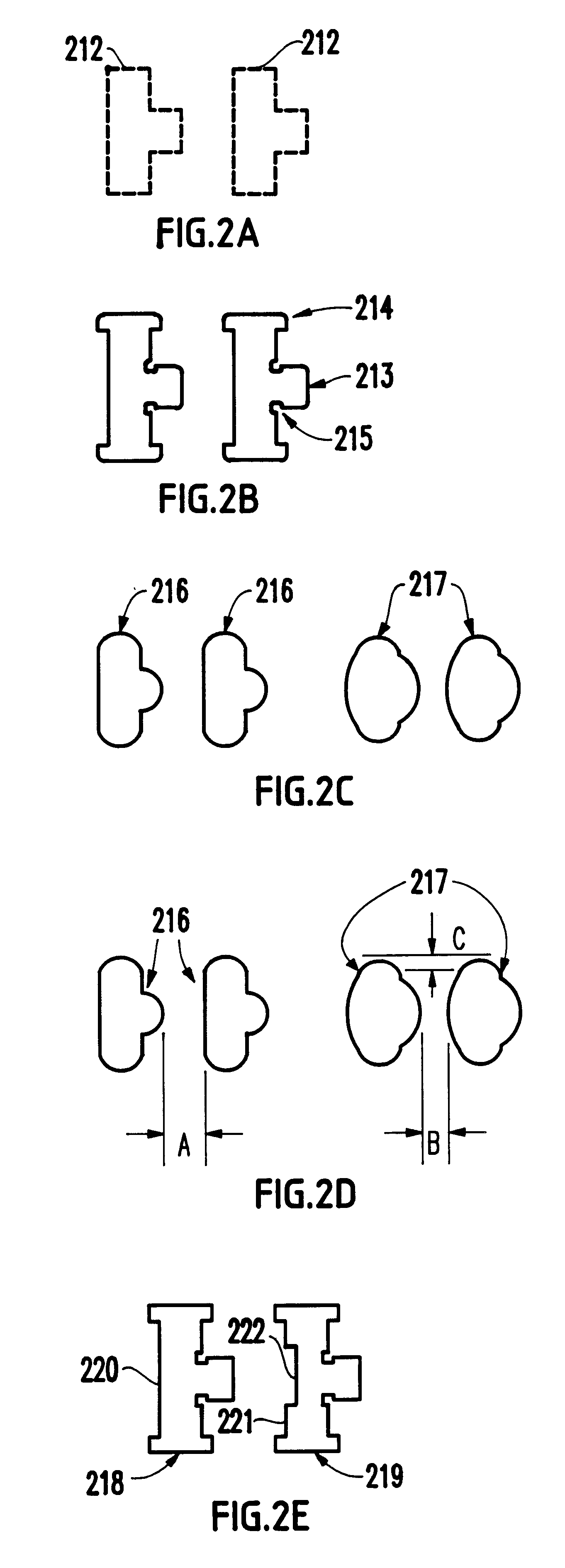
Referring now to the drawings, and more particularly to FIGS. 2A-2E and 3, a flowchart and the shapes produced by the processing in the flowchart are illustrated. As shown in FIGS. 2A and 3, input from a design manual 200 is used to create a design data set 201 of shapes 212. To initialize the program, this original data set 201 is designated a working design data set 202. Next, optical proximity corrections (OPC), aberration correction, and / or phase shift mask (PSM) adjustments, etc. are applied to the size, shape and spacing of the shapes 212 in step 203 to counteract the anticipated distortion that occurs during manufacturing, as shown in block 203. As discussed in the background section above, internal comers are notched 215 and external corners 214 may be extended with bars 213 to reduce anticipated distortions.

The working design data set 202 is subjected to shapes adjustment rules 204 which are intended to make changes to compensate for distortions introduced by the mask manuf...


PUM

PropertyMeasurementUnit
lengthsaaaaaaaaaa
sizeaaaaaaaaaa
shapeaaaaaaaaaa

Abstract

A method and computer system are provided for checking integrated circuit designs for design rule violations. The method may include generating a working design data set, creating a wafer image data set, comparing the wafer image data set to the design rules to produce an error list and automatically altering the working design data set when the comparing indicates a design rule violation. The method further automatically repeats the creating, the comparing and the automatically altering until no design rule violations occur or no solution to the errors exists.

Description

1. Field of the InventionThe present invention generally relates to modeling of integrated circuit layouts and more particularly to an improved process for checking for and correcting design rule violations.2. Description of the Related ArtConventional integrated circuit design rule checking systems check designed shapes against a complicated set of rules. More recently, design rule checking systems have begun to utilize commercial programs (such as those by Numerical Technologies, Inc., 333 West Maude Ave., Suite 207, Sunnyvale, Calif., U.S.A.), which model many of the diffraction induced phenomena and subsequently use the modeled wafer image as the input to a design rule checker. This approach simplifies the coding of the design rule checker since the complexities of the diffraction phenomena are accounted for in the wafer image modeling program. However, such conventional approaches do not account for photolithographic or other process effects on the net process window.As the min...

Claims


Application Information

Patent Timeline
Patent Type & Authority Patents(United States)
IPC IPC(8): G03F1/14G06F17/50G03F1/00G03F1/36
CPCG03F1/144G03F1/36G06F17/5081G06F30/398
Inventor BULA, ORESTCOLE, DANIEL C.CONRAD, EDWARD W.LEIPOLD, WILLIAM C.
Owner IBM CORP
Why Eureka
Try Eureka