Memory aliasing method and apparatus

a memory interface and aliasing technology, applied in the field of addressable memory interfaces, can solve the problems of user inability to remedy the above described problem, the access times of reasonably priced memory devices have not similarly improved, and the caching system described above suffers from significant drawbacks

Inactive Publication Date: 2002-08-20
AVAGO TECH INT SALES PTE LTD
View PDF29 Cites 28 Cited by
  • Summary
  • Abstract
  • Description
  • Claims
  • Application Information

AI Technical Summary

Problems solved by technology

While modern day processors have improved greatly in the Instruction execution time, access times of reasonably priced memory devices have not similarly improved.
While the use of cache memory in a memory/processor interface described above has provided a significant improvement in avoiding memory access time bottlenecks, and in preventing slow down of a processor otherwise capable of running at higher speed, the caching system described above suffers from significant drawbacks.
Unfortunately, conventional processor/memory interface architectures are fixedly defined by a system designer, thus a user cannot remedy the above described problem even if the user is aware of a set of information that is expected to be frequently referenced by the processor.
Unfortunately, faster speed cannot be easily realized in conventional processor/memory architectures because when the reduced sized program is referenced by the processor of the conventional system, portions of the program which may reference the common code segment are loaded into the cache.
Unfortunately, conventional architecture schemes do not account for the storage of the common code segm

Method used


Image

  • Memory aliasing method and apparatus
  • Memory aliasing method and apparatus
  • Memory aliasing method and apparatus

Examples


Embodiment Construction

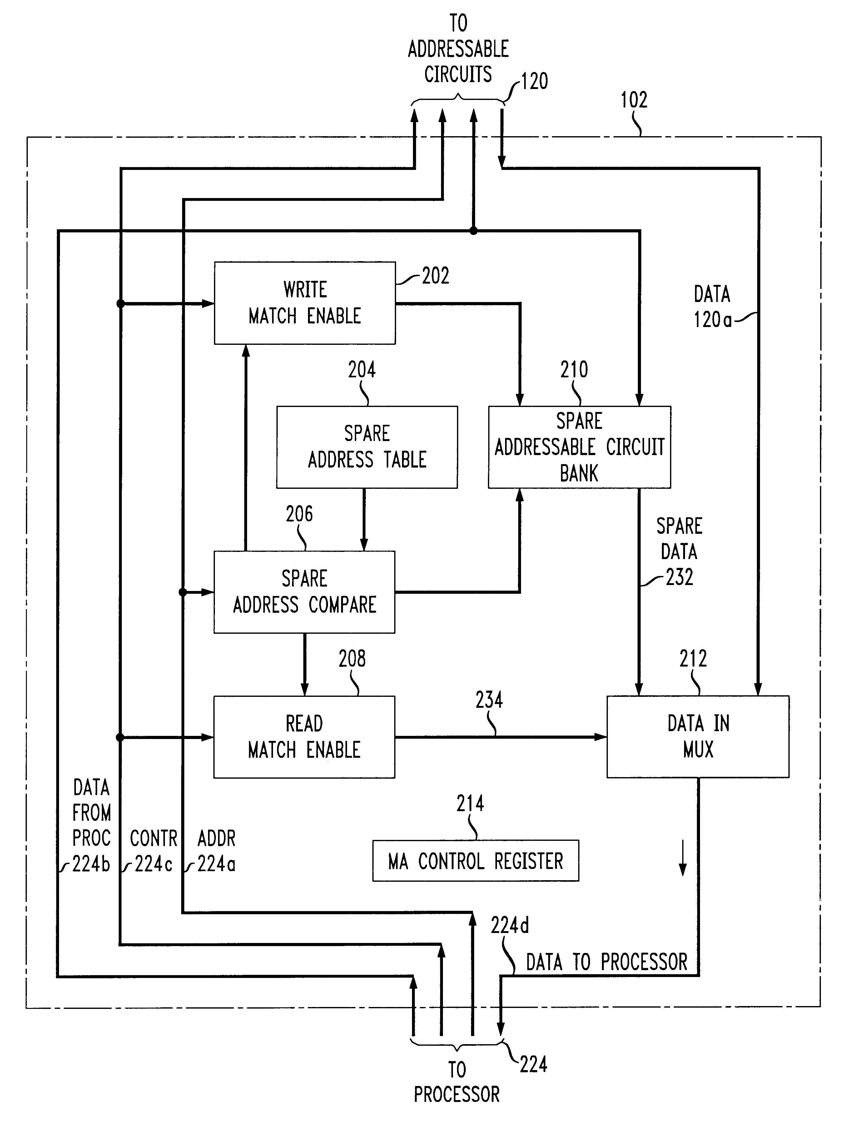
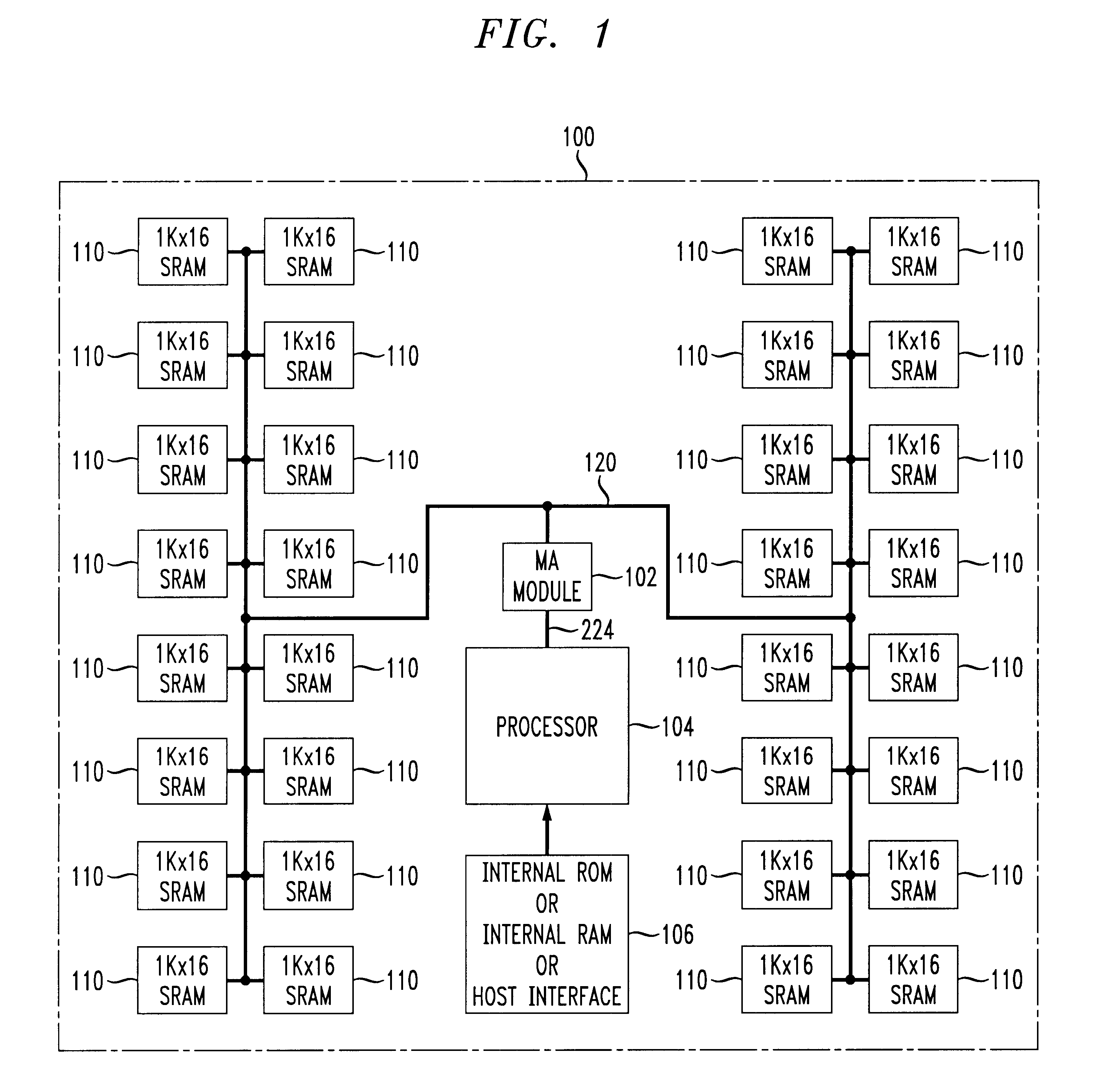
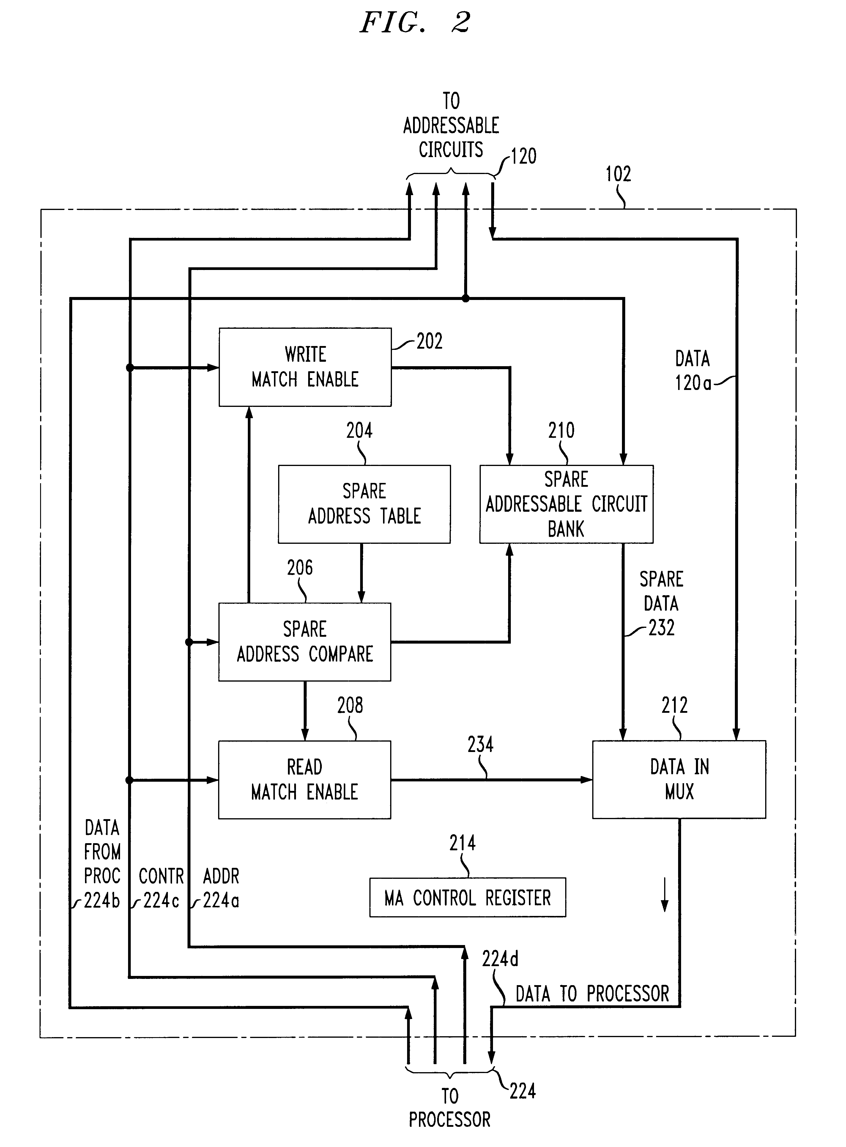
The present invention provides a flexible and efficient memory overlaying device usable with existing processor / memory architectures. A memory overlaying device in accordance with the principles of the present invention overlays user definable memory locations to reduce overall memory requirements. A memory overlaying device in accordance with the principles of the present invention is particularly useful for overlaying common global variables, common code segments and / or for user defined data.

While the present invention is described with respect to preferred embodiments in which an adaptive addressable circuit redundancy module is provided as an example of a memory aliasing module of the present invention, the present invention is equally applicable to any such device capable of overlaying memory locations for monitoring / snooping memory access by a processor.

The present invention provides an adaptive, flexible and efficient memory address overlaying method and apparatus for use in ...


PUM


Abstract

A flexible memory overlaying apparatus and method stores repeatedly referenced information, e.g, common global variables, common code segments, interrupt service routines, and/or any other user or system definable information, in spare addressable circuits accessed by a memory aliasing or overlaying module. The memory aliasing module monitors (or snoops) memory access by a processor to redirect access to certain appropriate addressable circuits to provide faster access to the information than would be available in an access made from main memory. The memory overlaying apparatus and method provides an efficient context switching, e.g., during an interrupt, enables a reduction in the size of instruction code requirements, and helps avoid the occurrences of cache misses, and/or thrashing between cached pages.

Description

1. Field of the InventionThis invention relates to a addressable memory interface. More particularly, it relates to a method and apparatus to adaptively overlay a group of memory addresses to provide an efficient and flexible processor / memory interface.2. Background of Related ArtProcessors nowadays are more powerful and faster than ever. So much so that even memory access time, typically in tens of nanoseconds, is seen as an impediment to a processor running at its full speed. Typical CPU time of a processor is the sum of the clock cycles executing instructions and the clock cycles used for memory access. While modern day processors have improved greatly in the Instruction execution time, access times of reasonably priced memory devices have not similarly improved.Thus, rather than relying on improvements in access speed of memory devices themselves, improved memory accessing methods and processor / memory interface architectures are employed in modern computer systems to minimize th...

Claims


Application Information

Patent Timeline
IPC IPC(8): G06F12/06G06F12/08G06F9/445G06F12/10
CPCG06F12/0638G06F12/0862
Inventor FISCHER, FREDERICK HARRISONSINDALOVSKY, VLADIMIRSEGAN, SCOTT A.
Owner AVAGO TECH INT SALES PTE LTD
Why Eureka
Try Eureka