Method and apparatus for optical film stack fault detection

a technology of optical film stack and fault detection method, which is applied in the direction of individual semiconductor device testing, semiconductor/solid-state device testing/measurement, instruments, etc., can solve the problems of difficult fault detection analysis and difficulty in tracking the characteristics of film stacks

Inactive Publication Date: 2002-10-01
GLOBALFOUNDRIES US INC
View PDF1 Cites 20 Cited by
  • Summary
  • Abstract
  • Description
  • Claims
  • Application Information

AI Technical Summary

Problems solved by technology

Due to the complexities of manufacturing facilities, tracking the characteristics of film stacks may be difficult.
However, without an accurate characterization of the film stack, an efficient fault detection analysis is difficult.

Method used


Image

  • Method and apparatus for optical film stack fault detection
  • Method and apparatus for optical film stack fault detection
  • Method and apparatus for optical film stack fault detection

Examples


Embodiment Construction

Illustrative embodiments of the invention are described below. In the interest of clarity, not all features of an actual implementation are described in this specification. It will of course be appreciated that in the development of any such actual embodiment, numerous implementation-specific decisions must be made to achieve the developers' specific goals, such as compliance with system-related and business-related constraints, which will vary from one implementation to another. Moreover, it will be appreciated that such a development effort might be complex and time-consuming, but would nevertheless be a routine undertaking for those of ordinary skill in the art having the benefit of this disclosure.

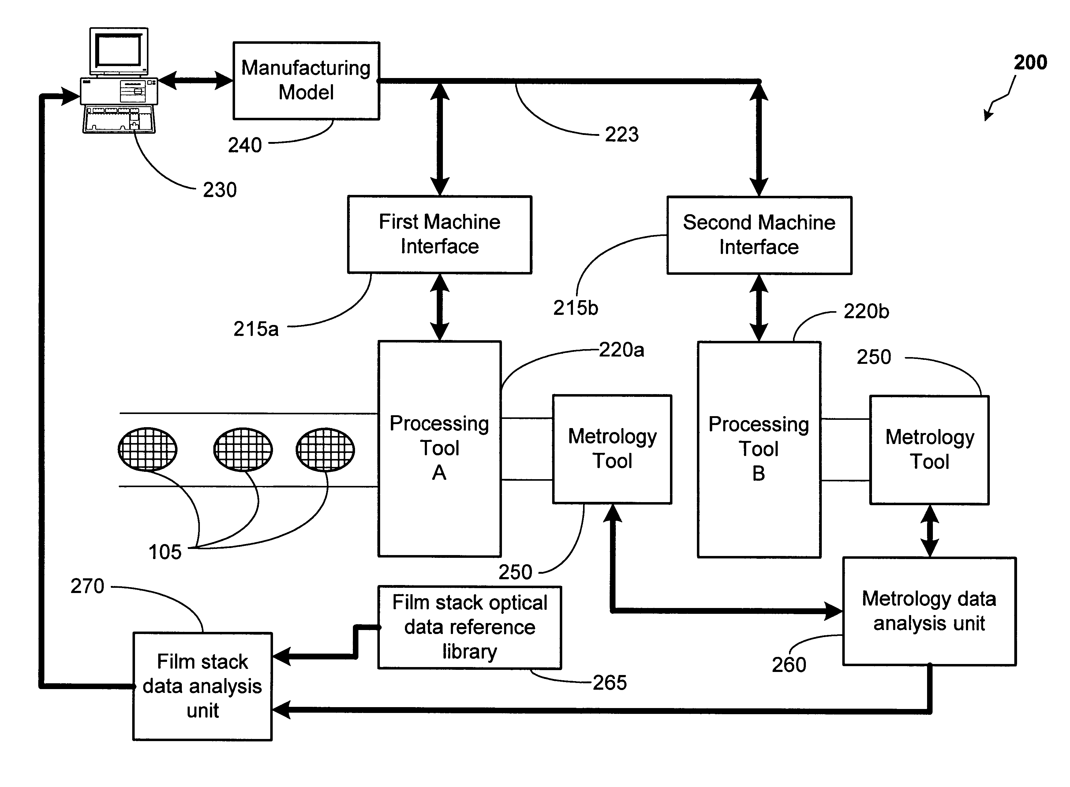
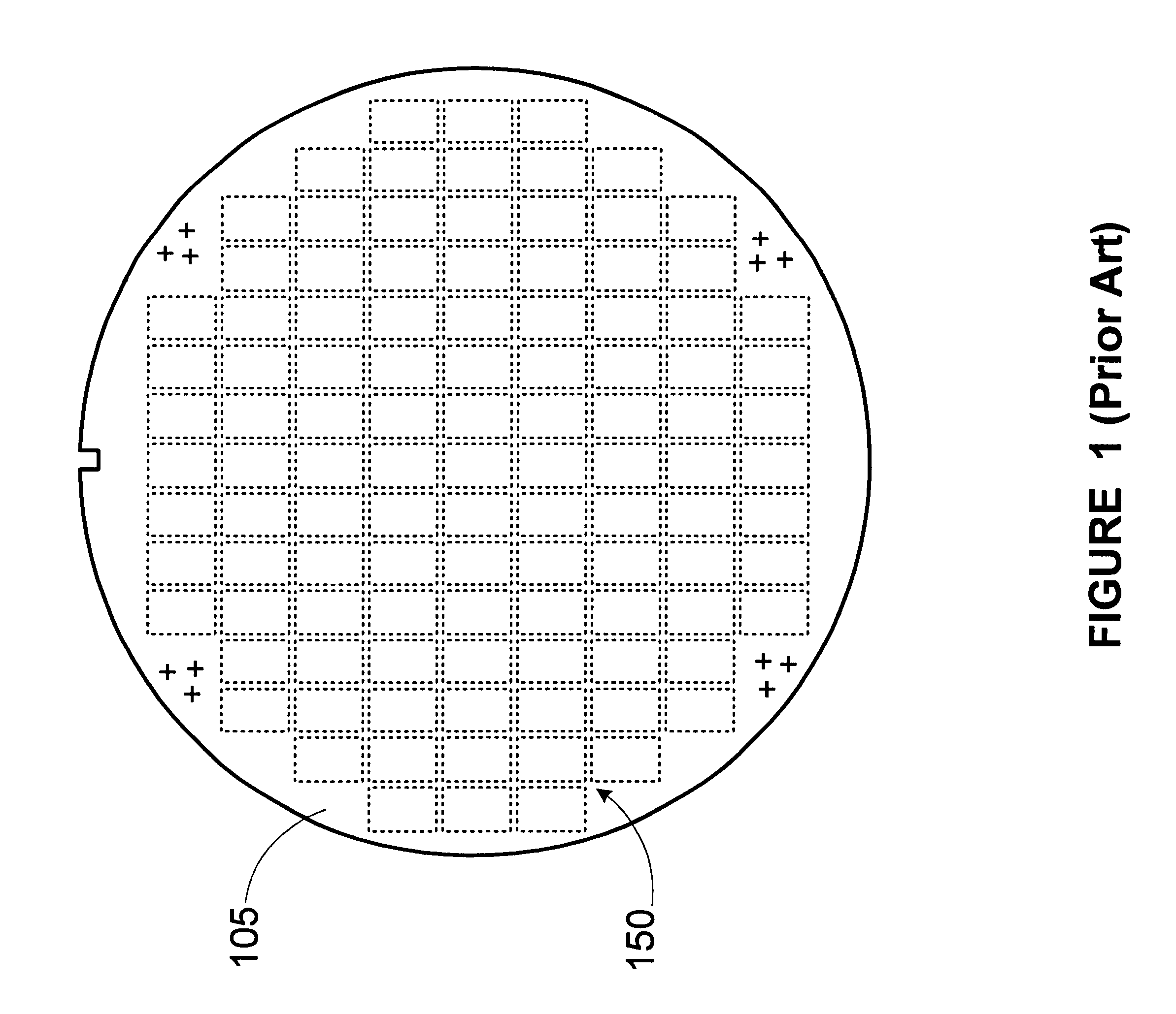
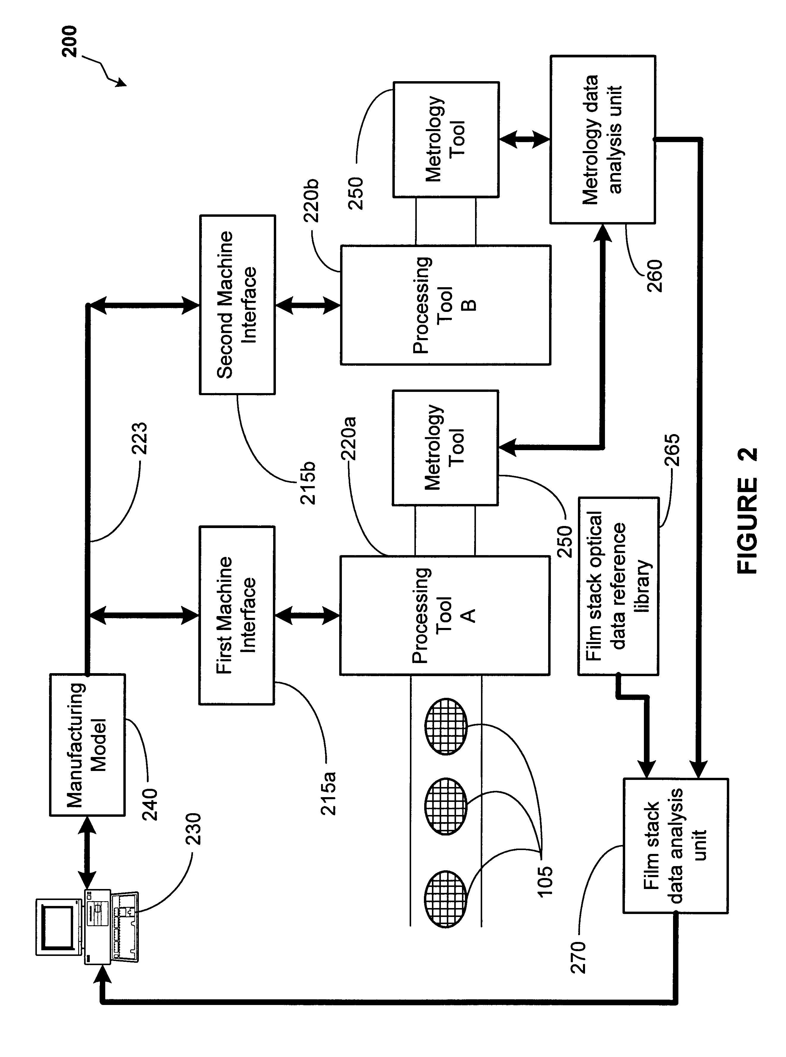
There are many discreet processes that are involved in semiconductor manufacturing. Many times, semiconductor devices are stepped through multiple manufacturing process tools. Errors that can occur during the formation of film stacks on semiconductor wafers being processed can cause si...


PUM

PropertyMeasurementUnit
thicknessaaaaaaaaaa
thicknessaaaaaaaaaa
thicknessaaaaaaaaaa

Abstract

A method and an apparatus for performing film stack fault detection. At least one semiconductor wafer is processed. Metrology data from the processed semiconductor wafer is acquired. Data from a reference library comprising optical data relating to a film stack on the semiconductor wafer is accessed. The metrology data is compared to data from the reference library. A fault-detection analysis is performed in response to the comparison of the metrology data and the reference library data.

Description

1. Field of the InventionThis invention relates generally to semiconductor manufacturing, and, more particularly, to a method and apparatus for performing film stack fault detection using optical data.2. Description of the Related ArtThe technology explosion in the manufacturing industry has resulted in many new and innovative manufacturing processes. Today's manufacturing processes, particularly semiconductor manufacturing processes, call for a large number of important steps. These process steps are usually vital, and therefore, require a number of inputs that are generally fine-tuned to maintain proper manufacturing control.The manufacture of semiconductor devices requires a number of discrete process steps to create a packaged semiconductor device from raw semiconductor material. The various processes, from the initial growth of the semiconductor material, the slicing of the semiconductor crystal into individual wafers, the fabrication stages (etching, doping, ion implanting, or...

Claims


Application Information

Patent Timeline
Patent Type & Authority Patents(United States)
IPC IPC(8): G01N21/956G01N21/88H01L21/66
CPCG01N21/95607H01L22/20H01L2223/54453
Inventor LENSING, KEVIN R.WRIGHT, MARILYN I.STIRTON, JAMES B.
Owner GLOBALFOUNDRIES US INC
Why Eureka
Try Eureka