
Method for producing a thin membrane and resulting structure with membrane

Inactive Publication Date: 2002-10-15
S O I TEC SILICON ON INSULATOR THECHNOLOGIES
View PDF37 Cites 67 Cited by
  • Summary
  • Abstract
  • Description
  • Claims
  • Application Information

AI Technical Summary

Benefits of technology

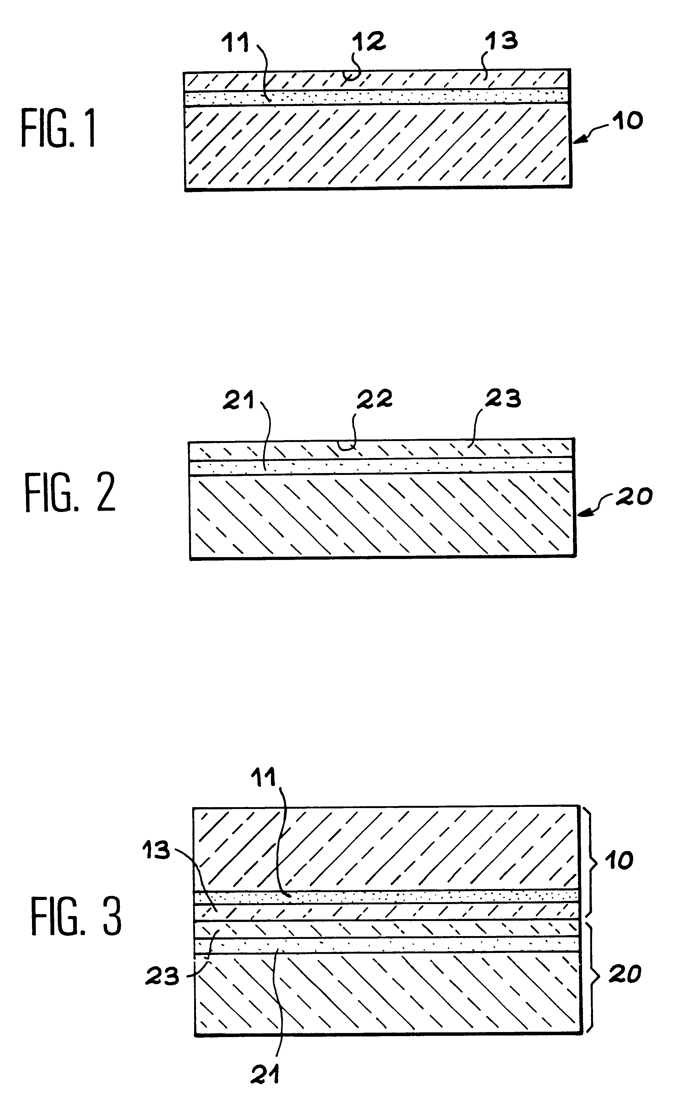
This assembly of the first substrate onto the second substrate may also be made by inserting an intermediate layer. The presence of an intermediate layer may modify the apparent rigidity of the membrane and modify transfer conditions. In particular, it may modify the annealing conditions and / or the mechanical fracture conditions.
If the detachment of a thin layer implies the application of heat treatment, the latter may be applied under controlled pressure (for example a gas or mechanical pressure). Lowering of the pressure at the time of heat treatment or at the time of separation may facilitate separation. In this way, it is possible to obtain separations at lower doses of implanted gas and / or lower heat treatments. By lower heat treatments is meant annealing conducted at a lower temperature and / or for a shorter time period. If pressure is increased, the fracturing conditions at the time separation occurs are modified and separation can be delayed. This delay may be advantageous in that it induces less surface roughness after fracturing but it may also enable fracturing to be obtained under conditions in which platelet formation is achieved with annealing at atmospheric pressure.

Problems solved by technology

With epitaxial growth the problem is raised of compatibility between the different layers.
These compatibility problems may for example relate to widely varying mesh parameters leading to dislocations in at least one of the layers.
On this account, some structures appear impossible to obtain.
However, with this method, it is impossible, depending upon the mechanical nature of the required film, to obtain self-supporting thin films using standard commercially available implanters, that is to say using implanters having a maximum implanting energy of 200 keV.
For example, it is impossible to obtain a silicon film having a thickness of 4 .mu.m with such energy.
Another problem is raised if it is desired to use a standard implanter (energy less than 200 keV) to transfer a thin film onto an ordinary support, that is to say a support which does not have sufficient rigidity to obtain a stiffening effect.

Method used


Image

  • Method for producing a thin membrane and resulting structure with membrane
  • Method for producing a thin membrane and resulting structure with membrane
  • Method for producing a thin membrane and resulting structure with membrane

Examples


Embodiment Construction

The substrates used to produce the thin layers may be solid or already comprise one or more thin layers deposited by epitaxy for example.

The implantation of gas species may be conducted, for each substrate, at different energies and doses. It may also be conducted using different gas species.

The fixing of the substrates onto one another may be made by bonding through molecular adhesion optionally with the presence of an intermediate layer which may have different functions. It may be chosen on account of its electronic and / or optic and / or mechanical and / or thermal properties. It may be insulating or conductive. Its mechanical properties may be chosen such as to rigidify the structure and enable a reduction in required thickness.

The separation of the thin layers with their substrates may be made in simultaneous or consecutive manner. Separation may be made using heat treatment and / or by means of mechanical forces applied simultaneously or after optional heat treatment. If the purpose...


PUM


Abstract

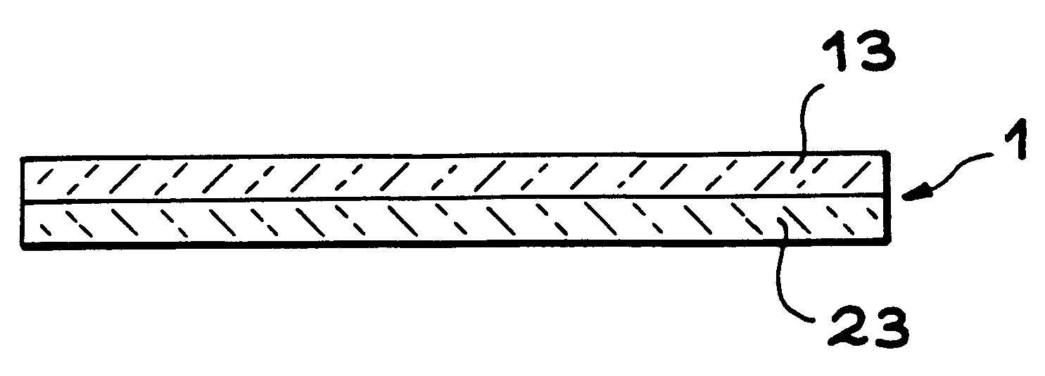
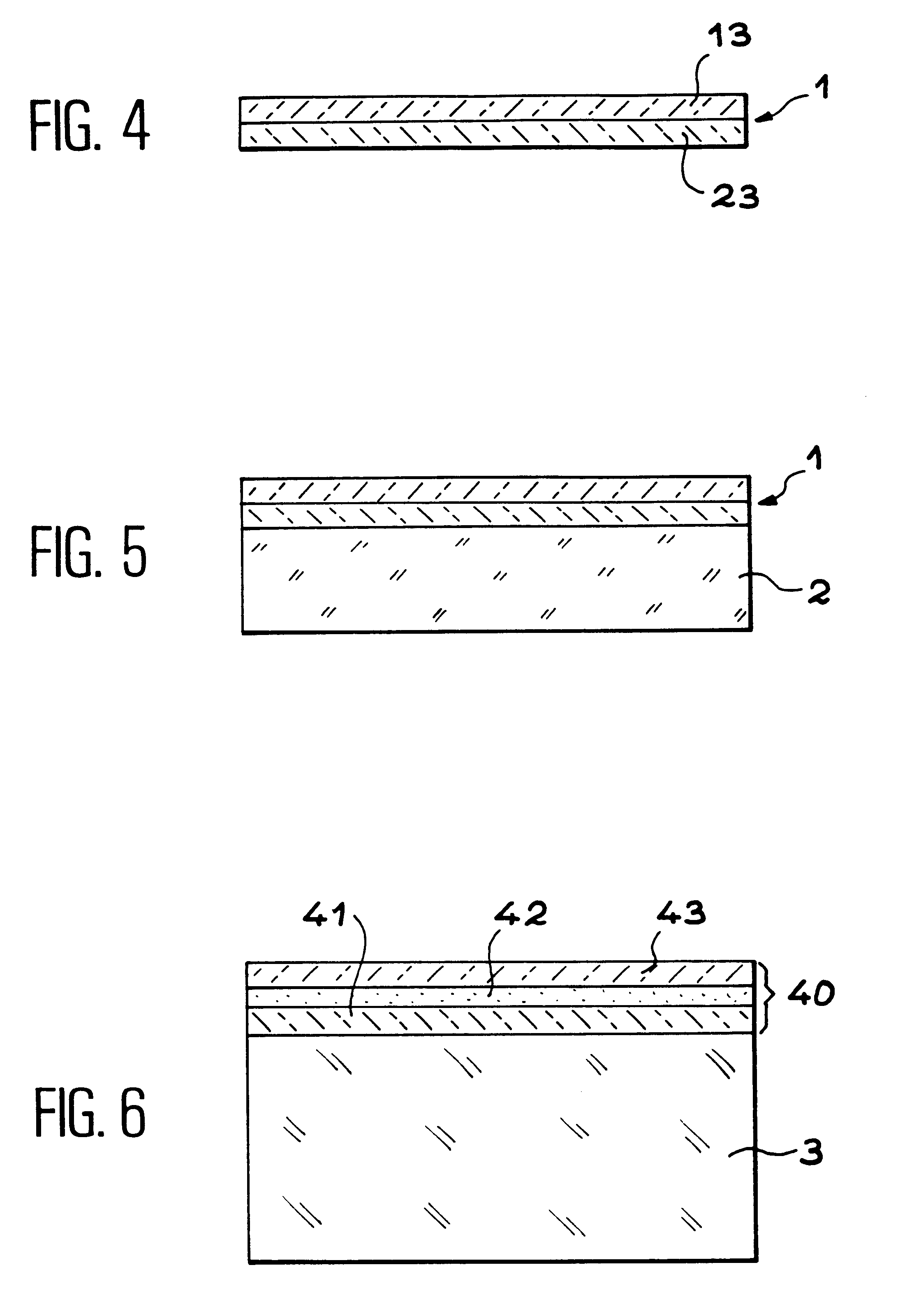
The invention relates to a method for producing a thin membrane, comprising the following steps:implanting gas species, through one surface of a first substrate (10) and through one surface of a second substrate (20), which in said substrates are able to create microcavities (11, 21) delimiting, for each substrate, a thin layer (13, 23) lying between these microcavities and the implanted surface, the microcavities being able, after their implantation, to cause detachment of the thin layer from its substrate;assembly of the first substrate (10) onto the second substrate (20) such that their implanted surfaces face one another;detaching each thin layer (13, 23) from its substrate (10, 20), the thin layers remaining assembled together to form said thin membrane.The invention also concerns a thin membrane structure obtained with this method.

Description

The present invention concerns a method for producing a thin membrane and the membrane structure so obtained. This membrane may be made up of one or more materials, monocrystalline materials in particular. It may be self-supporting or fixed to a supporting substrate to rigidify the structure so obtained.This type of membrane offers many advantages. By way of example, mention may be made of compliant substrates which may use a membrane of the invention, or any other application in which a thin film is required (silicon film on a glass or plastic substrate). By compliant substrate is meant a structure able to accept the stresses induced by a structure adhering to it, and which may be a layer deposited on a surface of this substrate by heteroepitaxy for example.PRIOR ARTFR-A-2 681 472 describes a method for fabricating thin films in semiconductor material. This document discloses that the implanting of a rare gas or of hydrogen into a substrate in semiconductor material is able to crea...

Claims


Application Information

Patent Timeline
IPC IPC(8): H01L21/20H01L21/02H01L27/12
CPCH01L21/2007H01L21/20
Inventor ASPAR, BERNARDBRUEL, MICHELJAUSSAUD, CLAUDELAGAHE, CHRYSTELLE
Owner S O I TEC SILICON ON INSULATOR THECHNOLOGIES
Learn More