Unmolded package for a semiconductor device

a semiconductor device and packaging technology, applied in the field of packaging for semiconductor devices, can solve problems such as complicated manufacturing (packaging) processes

Inactive Publication Date: 2002-10-22
SEMICON COMPONENTS IND LLC
View PDF3 Cites 123 Cited by
  • Summary
  • Abstract
  • Description
  • Claims
  • Application Information

AI Technical Summary

Problems solved by technology

These prior art concepts involve various components and may result in complicated manufacturing (packaging) processes.

Method used


Image

  • Unmolded package for a semiconductor device
  • Unmolded package for a semiconductor device
  • Unmolded package for a semiconductor device

Examples


Embodiment Construction

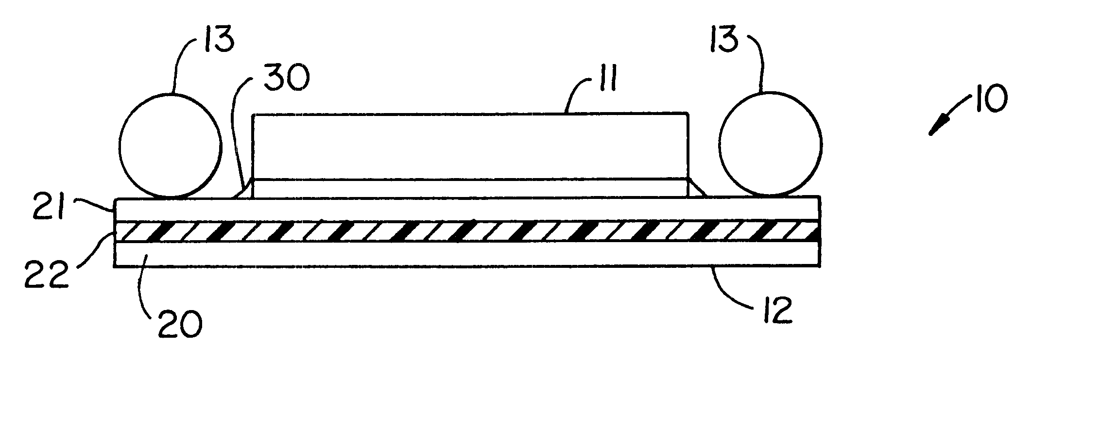
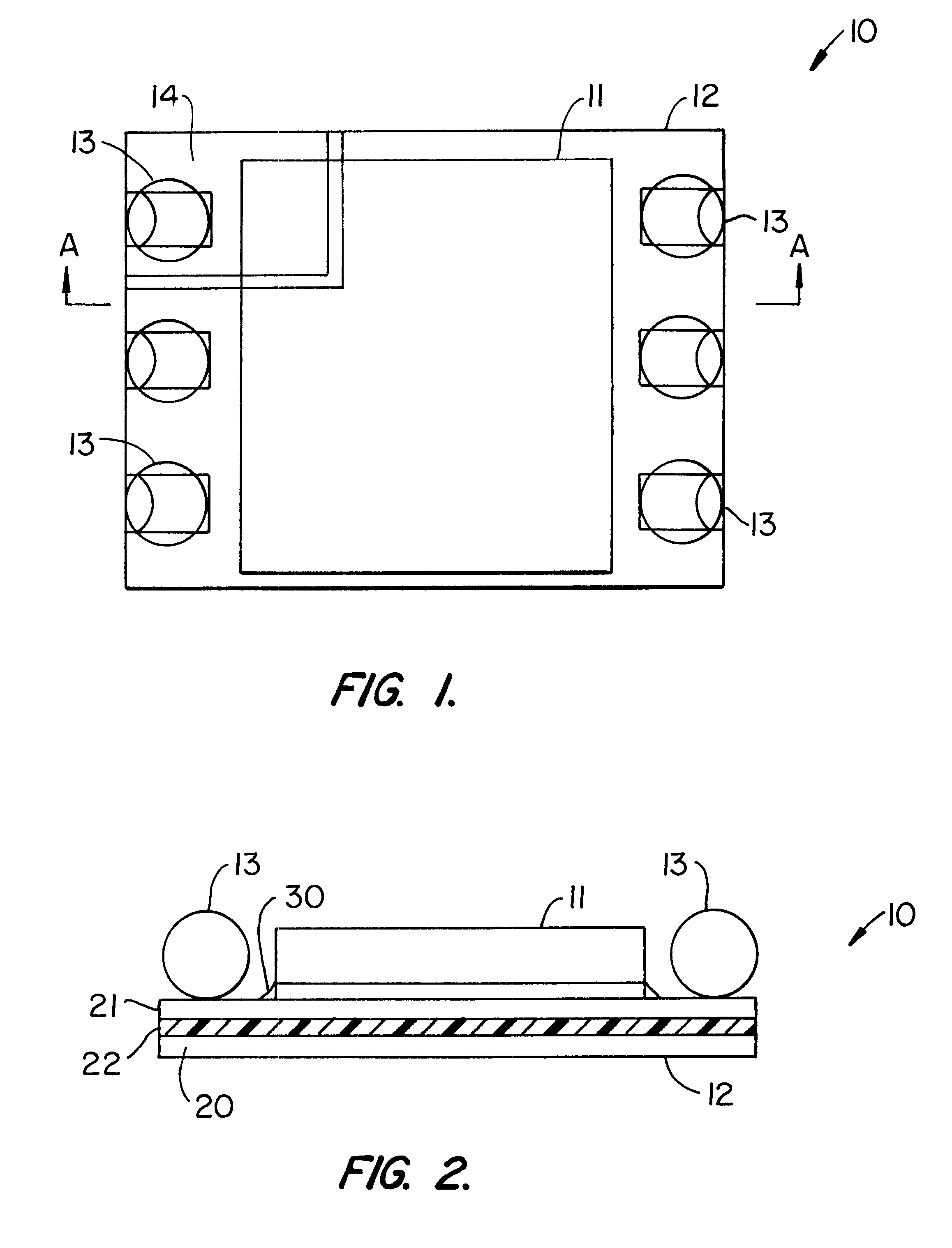
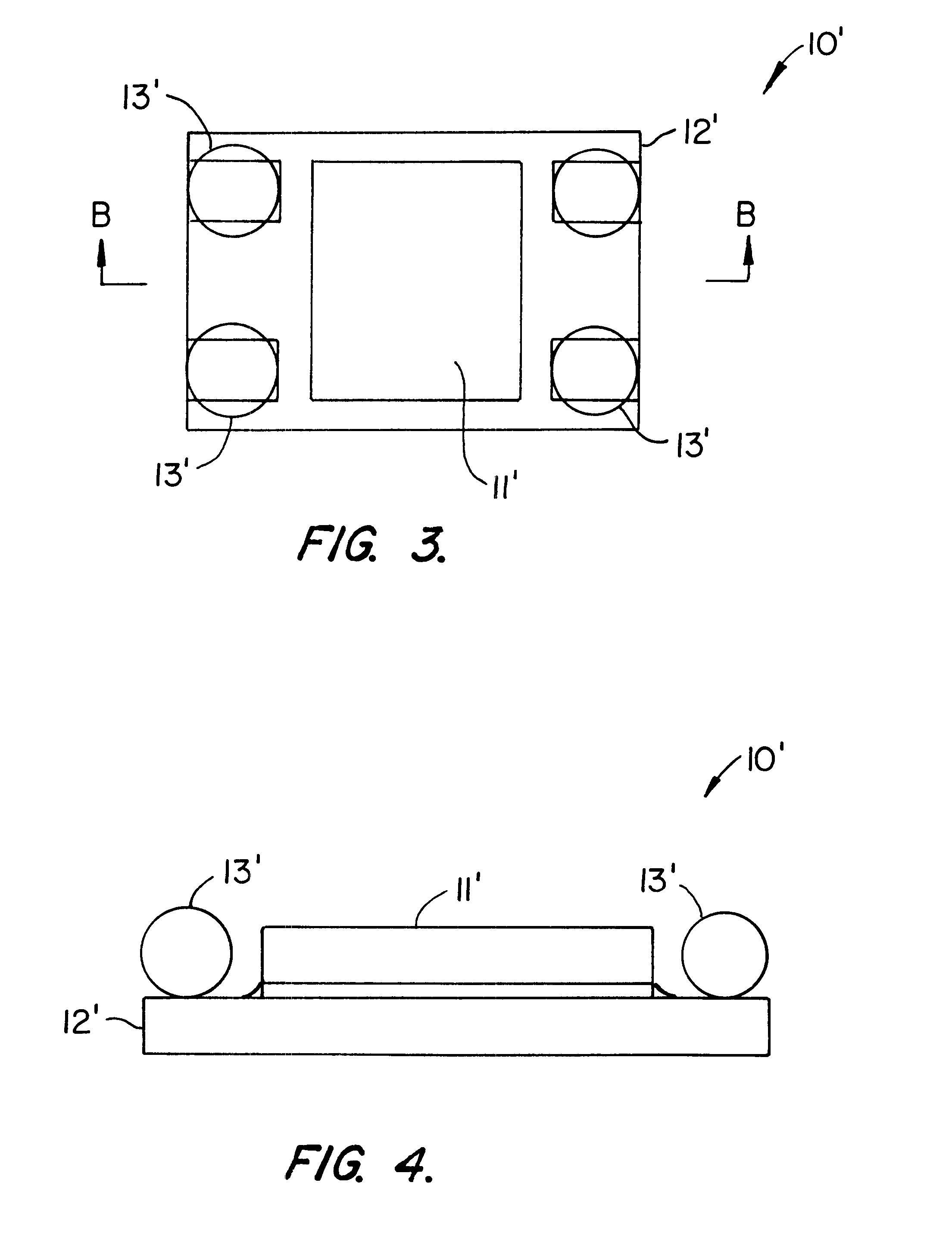
FIG. 1 illustrates a MOSFET semiconductor device 10 that includes a die 11, a substrate 12 and solder balls 13. The substrate includes a gate region 14.

As can be seen in FIG. 2, the substrate preferably comprises a base layer 20 and a top, metal layer 21. The base layer and the top metal layer are separated by an insulting layer 22, preferably an insulating epoxy that joins the two layers. The base material preferably comprises a metallized pattern while the top metal layer preferably comprises another metallized pattern. The metal layer may also serve as a heat spreader.

The die is preferably coupled to the substrate with high temperature solder paste, but may also be coupled with any other suitable conductive interconnect known in the art. The solder balls are placed adjacent the die on opposite sides of the die, with at least one solder ball being placed on the gate region of the substrate.

Thus, in use, the semiconductor device is placed on a printed circuit board and the surface ...


PUM


Abstract

A semiconductor device that does not include a molded body or package. The semiconductor device includes a substrate and a die coupled to the substrate. The die is coupled to the substrate such that the source and gate regions of the die, assuming a MOSFET-type device, are coupled to the substrate. Solder balls are provided adjacent to the die such that when the semiconductor device is coupled to a printed circuit board, the exposed surface of the serves as the drain connections while the solder balls serve as the source and gate connections.

Description

1. Field of the InventionThe present invention relates to a package for a semiconductor device, and more particularly, to a package for a semiconductor device that does not require a molded body.2. Description of the Prior ArtSemiconductor devices, especially MOSFET devices, generally desire very low package resistance (RDSon) with good thermal performance. It is also generally desirable to have simple, quick and efficient methods of packaging semiconductor devices. Thus, numerous packaging concepts and methods have been developed in the prior art.An example of one such packaging concept involves a ball grid array (BGA). Such a concept involves an array of source, gate and drain solder balls that are connected directly to the printed circuit board (PCB). This requires a bumped die and a leadframe is used to facilitate the drain contact. Another packaging concept is commonly referred to as Flip Chip in Leaded Molded Package (FLMP), which comprises a molded leaded surface mount packag...

Claims


Application Information

Patent Timeline
Patent Type & Authority Patents(United States)
IPC IPC(8): H01L23/48H01L23/498H01L23/12H01L21/60H01L23/14H01L23/373H01L23/538H01L25/065H01L25/07H01L25/18H05K3/34
CPCH01L23/145H01L23/3735H01L23/49816H01L23/5383H01L25/074H01L2924/15311H01L2924/1532H05K3/3436H01L24/48H01L2224/16227H01L2224/48227H01L2924/13091H01L2924/15321H01L2224/16225H01L24/45H01L2224/451H01L2224/45147H01L2924/181H01L2924/00H01L2924/00015
Inventor JOSHI, RAJEEV
Owner SEMICON COMPONENTS IND LLC
Why Eureka
Try Eureka