Method for producing semiconductor device

a technology of semiconductor devices and thin films, applied in the direction of semiconductor devices, basic electric elements, electrical apparatus, etc., can solve the problems of inability to constitute peripheral driver circuits inability to meet the required level of characteristics of tfts utilizing amorphous silicon thin films, and inability to achieve the effect of peripheral driver circuits

Inactive Publication Date: 2002-11-12
SEMICON ENERGY LAB CO LTD
View PDF30 Cites 51 Cited by
  • Summary
  • Abstract
  • Description
  • Claims
  • Application Information

AI Technical Summary

Problems solved by technology

However, TFTs based on thin films of amorphous silicon are still inferior in performance.
If a higher display function is required as a liquid crystal display of an active matrix type, the characteristics of TFTs utilizing an amorphous silicon film are too low to satisfy the required level.
However, a TFT using an amorphous silicon thin film cannot constitute a peripheral driver circuit because of its low operation speed.
In particular, a basic problem is that a CMOS circuit is unavailable from a amorphous silicon thin film.
This is due to the difficulty in implementing a practical P-channel type TFT by using amorphous silicon thin film (i.e., the TFT using an amorphous silicon thin film is practically unfeasible due to its too low performance).
However, a TFT using a thin film of amorphous silicon is too inferior in characteristics to constitute an integrated circuit capable of processing image data.
Hence, various problems arise due to the presence of grain boundaries.
For example, carriers which move through the grain boundaries greatly limit the withstand voltage of the TFT.
The change or degradation in characteristics which occurs in high speed operation is another problem.
However, even if the channel width should be extended, a TFT using a crystalline silicon film cannot be put into practice because of the problems of withstand voltage.
The large fluctuation in threshold voltage is another hindrance in making the TFT practically feasible.
A TFT using a crystalline silicon film cannot be applied to an integrated circuit for processing image data because of problems concerning the fluctuation in threshold voltage and the change in characteristics with passage of time.
Accordingly, a practically feasible integrated circuit based on the TFTs which can be used in place of conventional ICs cannot be realized.
In heat treatment, crystal growth cannot be performed within a desired area.
In this method, it is difficult to precisely control the concentration of the metal element to be introduced into the amorphous silicon film.
), it becomes difficult to form a film in a complete form.
However, in practice, MBE is only applicable to a limited area.
These recombination centers induce particularly undesirable characteristics such as an increase in leak current of the TFT.
However, this method using CVD is disadvantageous in that it is not as simple as the one using a solution.

Method used


Image

  • Method for producing semiconductor device
  • Method for producing semiconductor device
  • Method for producing semiconductor device

Examples


example 2

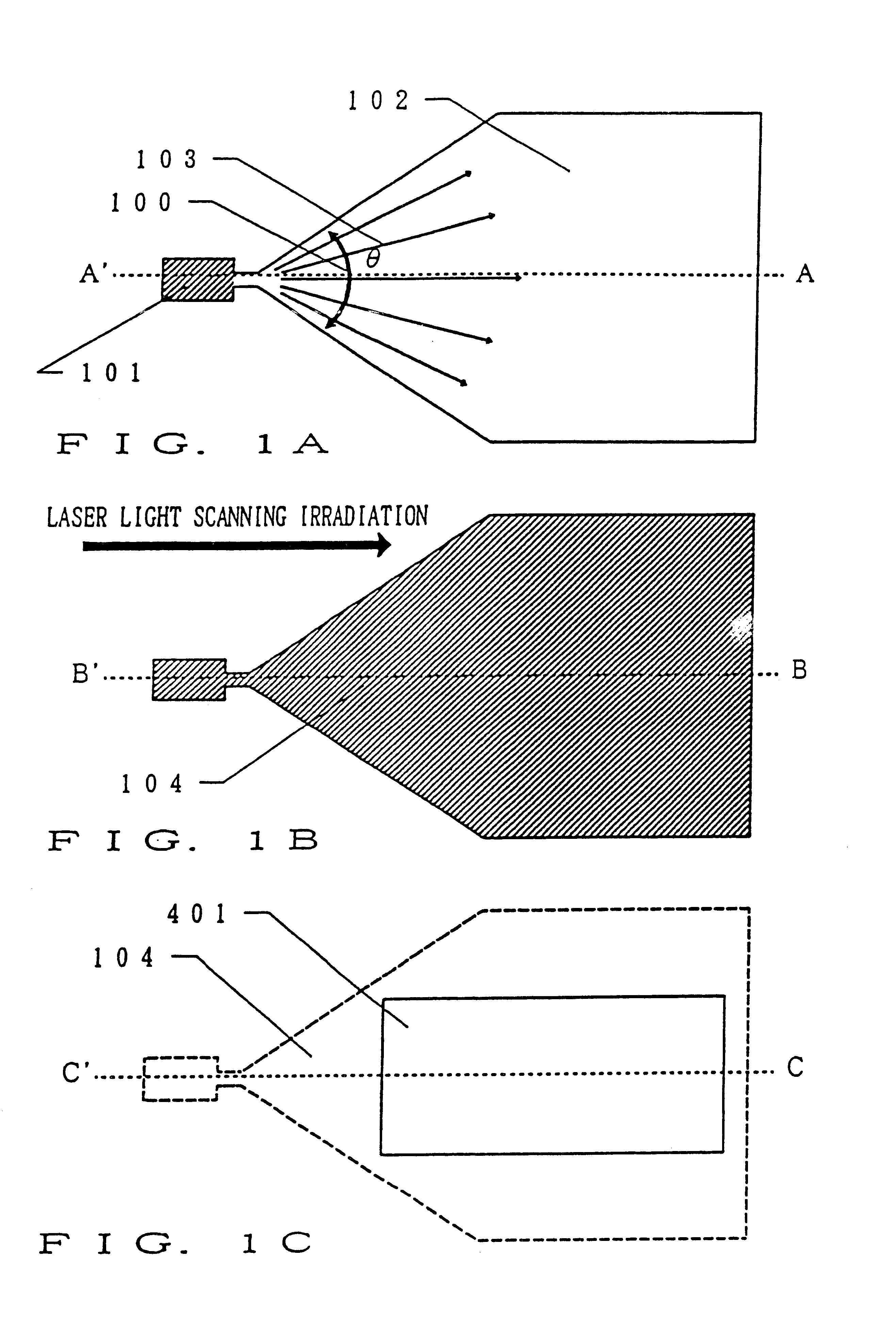
The present example refers to a method for manufacturing a thin film transistor (TFT) using a region equivalent to single crystal 104 as shown in FIGS. 3A to 3E. In FIGS. 4A to 4D, the method for producing a TFT according to the example is described. In FIG. 1C and FIG. 4A, the region equivalent to a single crystal 104 is patterned to form an active layer 401 for the TFT.

The cross sectional view taken along C-C' in FIG. 1C is given in FIG. 4A. In FIG. 4B, a silicon oxide film 402 is formed at a thickness of 1,000 .ANG. to provide a gate insulating film which covers the active layer 401. Then, a film based on aluminum and containing scandium is formed at a thickness of 7,000 .ANG. by electron beam vapor deposition, and the resulting film is patterned to form a gate electrode 403. After forming the gate electrode 403, anodic oxidation is effected in an electrolytic solution using the gate electrode 403 as the anode, to from an oxide layer 404 (FIG. 4B).

An impurity region is formed by ...

example 3

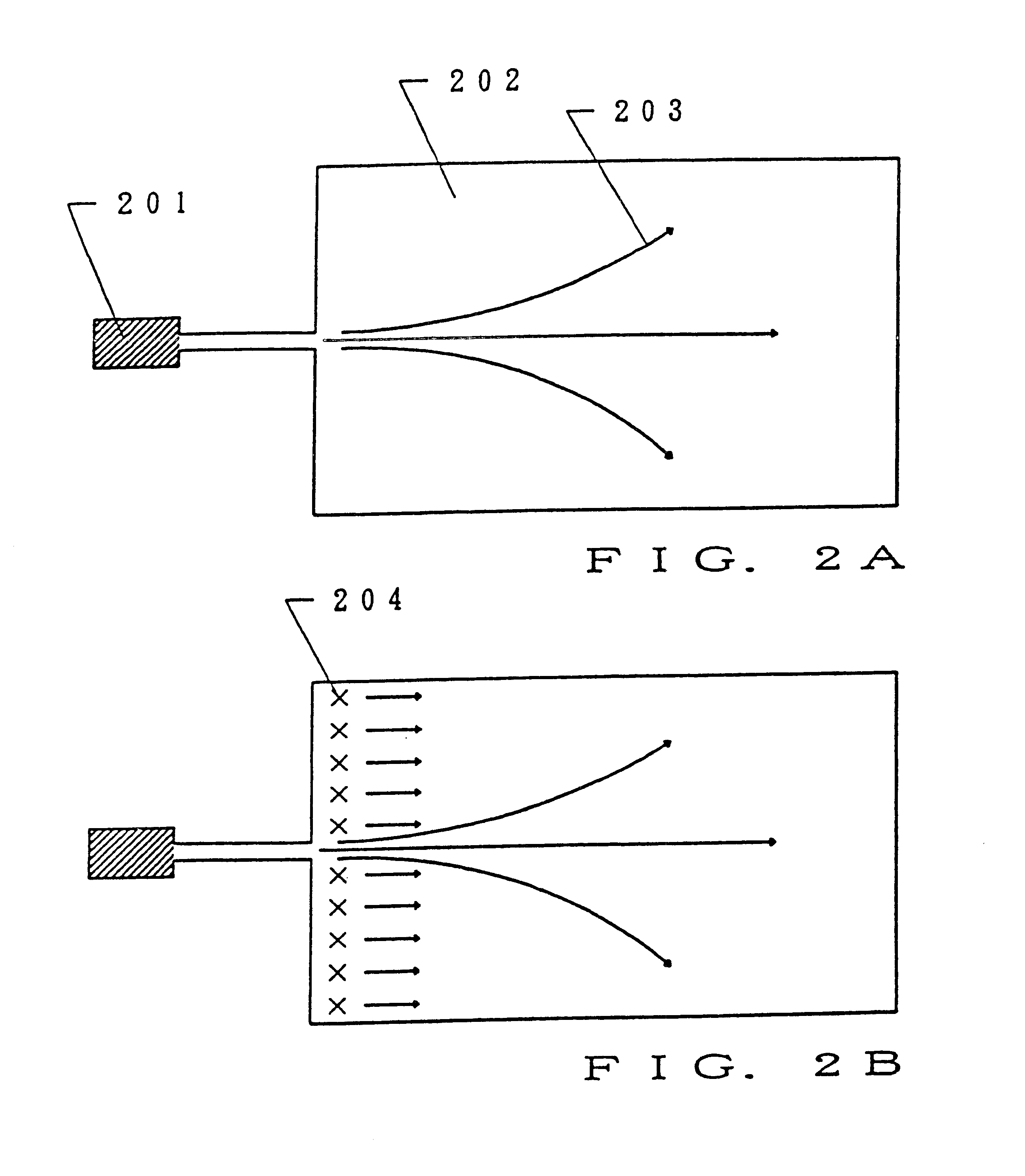
The present example refers to a method of forming a region equivalent to a single crystal (a monodomain region) by heating and allowing crystal growth to occur by utilizing a metal element which accelerates the crystallization of silicon, and further irradiating a laser light to the crystallized region. The steps for the present example are shown in FIGS. 5A and 5B and in FIGS. 6A and 6B. An amorphous silicon film (not shown in the figure) is formed to a thickness of 500 .ANG. by plasma CVD or low pressure thermal CVD. Although not shown in the figure, a glass substrate having a silicon oxide film formed on the surface thereof is used as the substrate.

A nickel layer or a layer containing nickel is formed by adding the substrate to a nickel acetate solution. The resulting substrate is patterned to form a region 502 (a square region with a length of 3 .mu.m). By thermal treatment at 550.degree. C. for 4 hours, the region 502 is crystallized to provide the seeds for crystal growth. Sin...

example 4

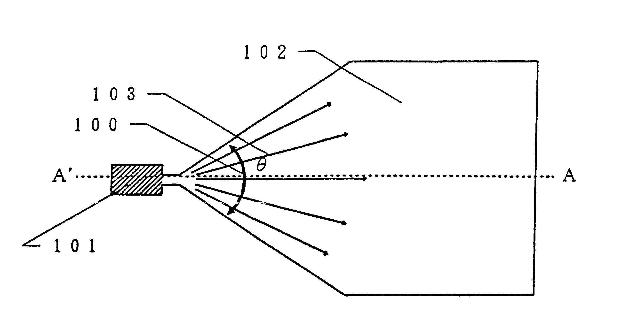
The present example relates to the shape of the patterns of a region equivalent to a single crystal (monodomain region) 102 and 505 shown in FIG. 1A and FIG. 6B. The patterns of the regions 102 and 505 are characterized in that the area thereof gradually increases in the direction of crystal growth. The particular patterns are provided to prevent crystal growth from occurring from a plurality of regions during crystal growth . If crystal growth proceeds from a plurality of regions, the growing crystals collide with each other to form grain boundaries. In other words, a uniform crystal growth can be effected by gradually extending the crystal growth from a single starting point; that is, the crystal growth is effected unimodal to form a region equivalent to a single crystal.

A uniform crystal growth can be effected by initiating crystal growth from a starting point, and gradually enlarging the region of crystal growth. In FIGS. 1A and 6B, the area of crystal growth gradually increases...


PUM

PropertyMeasurementUnit
temperatureaaaaaaaaaa
thicknessaaaaaaaaaa
thicknessaaaaaaaaaa

Abstract

In producing a thin film transistor, after an amorphous silicon film is formed on a substrate, a nickel silicide layer is formed by spin coating with a solution (nickel acetate solution) containing nickel as the metal element which accelerates (promotes) the crystallization of silicon and by heat treating. The nickel silicide layer is selectively patterned to form island-like nickel silicide layer. The amorphous silicon film is patterned. A laser light is irradiated while moving the laser, so that crystal growth occurs from the region in which the nickel silicide layer is formed and a region equivalent to a single crystal (a monodomain region) is obtained.

Description

1. Field of the InventionThe present invention relates to a method for producing a semiconductor device using a crystalline thin film semiconductor.2. Description of the Related ArtRecently, much attention is paid on a transistor constructed of a thin film semiconductor formed on a glass or quartz substrate. Such a thin film transistor (TFT) is constructed of a thin film semiconductor having a thickness of several hundreds to several thousands of angstroms (.ANG.), formed on the surface of a glass substrate or a quartz substrate (insulated gate field effect transistor).TFTs are used in an application field such as the field of an active matrix type liquid crystal display device. An active matrix type liquid crystal display device has several hundred thousands of pixels arranged in a matrix, and TFTs are provided to each of the pixels as switching elements to realize a high quality image display. Practically available TFTs designed for active matrix type liquid crystal display device...

Claims


Application Information

Patent Timeline
Patent Type & Authority Patents(United States)
IPC IPC(8): H01L21/02H01L21/20H01L21/336H01L21/423
CPCH01L21/2026H01L21/423H01L29/66757H01L21/02686H01L21/02488H01L21/02678H01L21/02422H01L21/02532H01L21/0242H01L21/02672H01L21/02691H01L21/02675
Inventor NAKAJIMA, SETSUOYAMAZAKI, SHUNPEIKUSUMOTO, NAOTOTERAMOTO, SATOSHI
Owner SEMICON ENERGY LAB CO LTD
Why Eureka
Try Eureka