Method and apparatus for reverse engineering integrated circuits by monitoring optical emission

a technology of optical emission and reverse engineering, applied in the direction of electronic circuit testing, measurement devices, instruments, etc., can solve the problems of destructive integrated circuit (ic) chips, difficult to use ic chips afterwards, and art methods that involve significant manual intervention by technical personnel

Inactive Publication Date: 2002-12-17
IBM CORP
View PDF3 Cites 46 Cited by
  • Summary
  • Abstract
  • Description
  • Claims
  • Application Information

AI Technical Summary

Problems solved by technology

Conventional methods of reverse engineering are usually physical methods that are often destructive of an integrated circuit (IC) chip.
Often these methods require unpackaging, and sometimes at least partially dissecting, the IC chip, making it very difficult to use the IC chip afterwards.
Further, these prior art methods typically involve significant manual intervention by technical personnel.
In the case of static memory circuits such as Flash ROM, these prior art methods are incapable of detecting the contents of the memory.
In addition, the methods can be tedious and inefficient.
Therefore, they usually cannot provide information about either the physical location of subcircuits of the chip or the device-level schematic of the transistors comprising each subcircuit.
Consequently, reverse engineering a complex IC chip without spatial information about specific devices that are in close proximity to each other on the IC chip can be very difficult with these methods.
Additionally, conventional techniques are readily defeated by a number of simple countermeasures that are well known.
However, the inability to probe more than a single device simultaneously can make reverse engineering by any single point probe method extremely time consuming, and hence, impractical.
In addition, with modern "flip-chip" ICs, preparing the chip for probing may require depackaging and removal of passivation or wiring layers, and is essentially destructive of the chip.

Method used


Image

  • Method and apparatus for reverse engineering integrated circuits by monitoring optical emission
  • Method and apparatus for reverse engineering integrated circuits by monitoring optical emission
  • Method and apparatus for reverse engineering integrated circuits by monitoring optical emission

Examples


Embodiment Construction

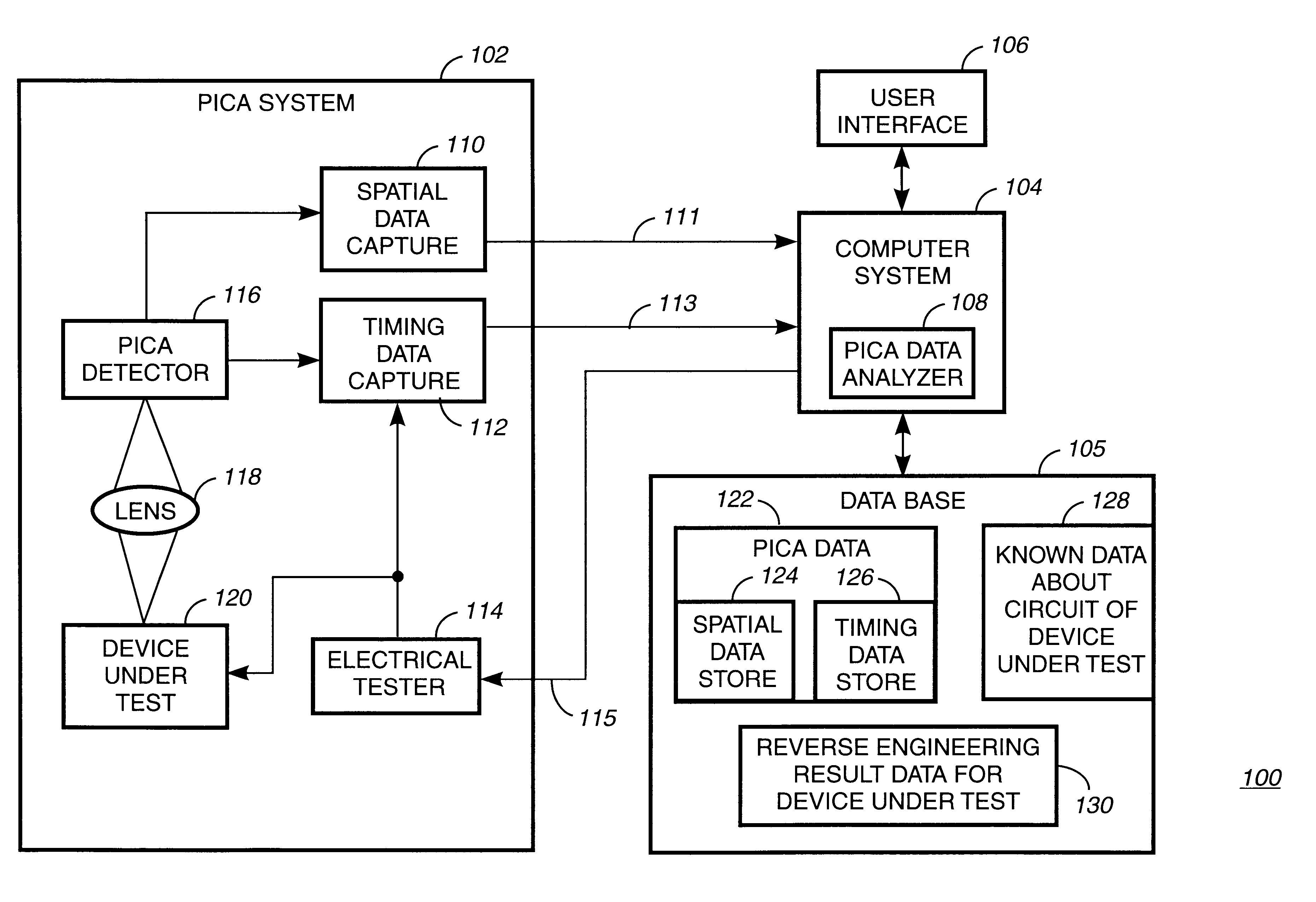
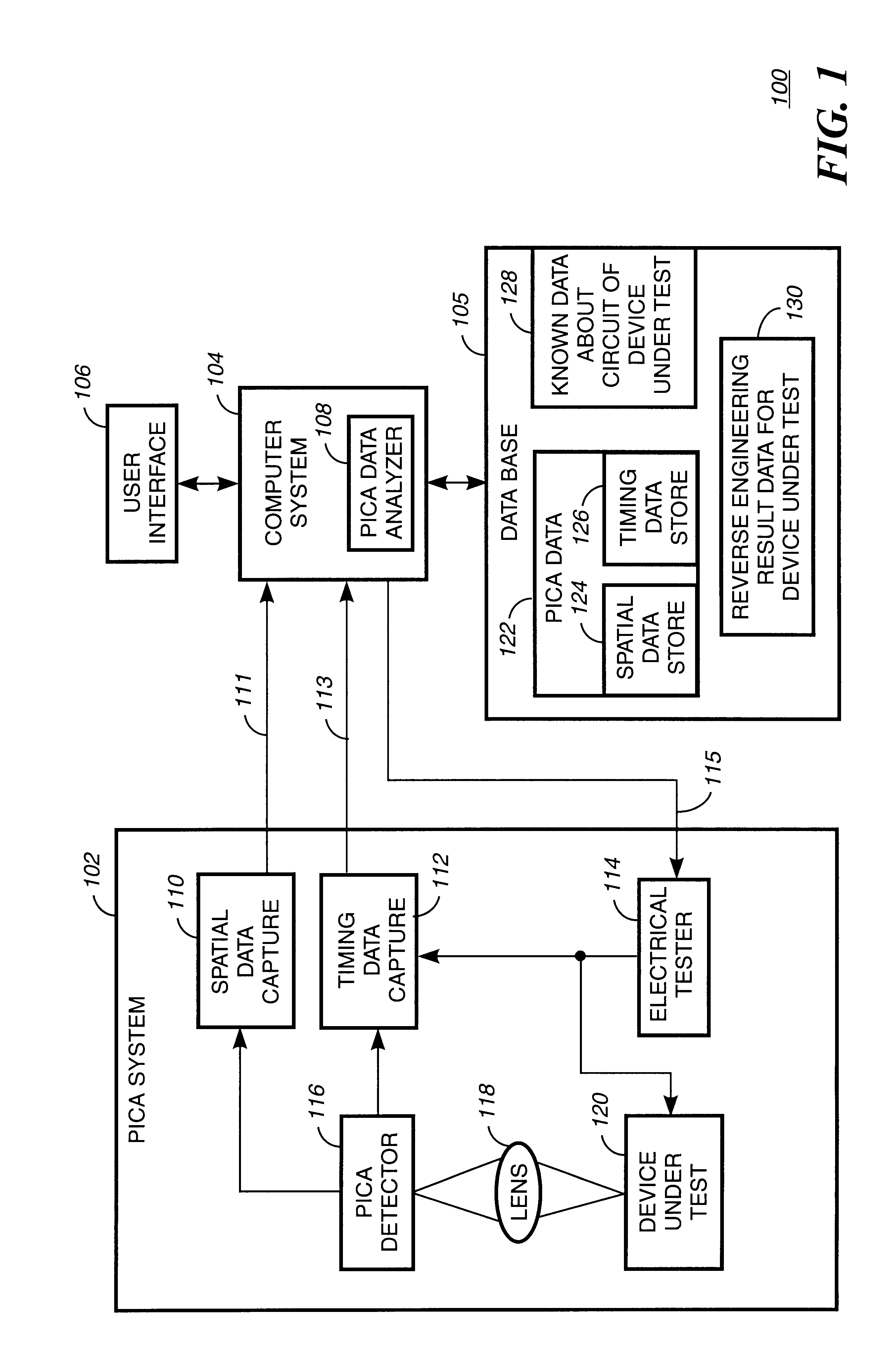
The present invention allows non-destructive reverse engineering by monitoring induced light emissions from active elements in an integrated circuit (IC) chip. Generally, light emissions from active elements can be monitored using methods and apparatus that have been taught in the following identified co-pending patent applications, the first one being numbered 08 / 683,837, entitled "Noninvasive optical method for measuring internal switching and other dynamic parameters of CMOS circuits", filed on Jul. 18, 1996, by inventors Kash et al., and the second one being numbered 09 / 026,063, entitled "System and method for compressing analyzing time-resolved optical data obtained from operating integrated circuits", filed on Feb. 19, 1998, by inventors Kash et al., and which are both owned by the assignee of the present invention, and the teachings of which are incorporated herein by reference.

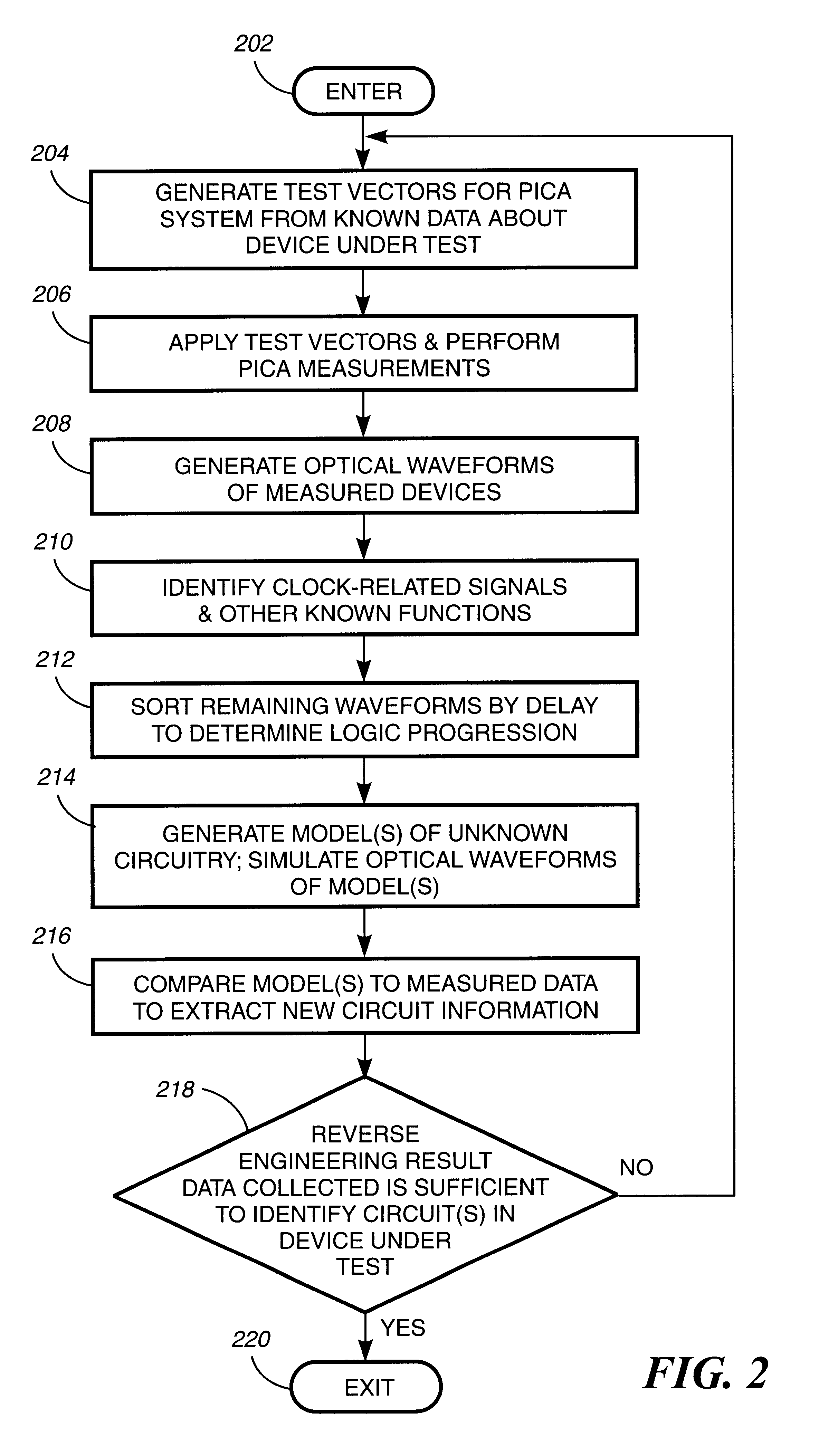
For effective reverse engineering of an IC chip, one would use advance knowledge of the integrated ...


PUM


Abstract

A method and apparatus for reverse engineering an integrated circuit chip (IC chip) (120) utilizes an electrical circuit tester (114) for injecting a triggering signal into the IC chip (120) to exercise a circuit under test. In synchronization thereto, a PICA detector (116) monitors optical emissions from the circuit under test. A spatial data extractor, electrically coupled to the PICA detector, collects space information (124) from patterns of light emissions emitted by the circuit under test, and a timing data extractor, electrically coupled to the electrical circuit tester and to the PICA detector (116), collects time information (126) from the patterns of light emissions emitted by the circuit under test. A database memory (105) includes known data about the circuit under test and also includes at least one reference pattern for comparing a captured light emission pattern thereto to identify at least one circuit element in the circuit under test. A PICA data analyzer (108), electrically coupled to the database memory (105) and to the PICA detector (116), determines at least one of whether the circuit under test comprises a circuit element with a light emission pattern that matches one of the at least one reference pattern in the database memory (105), and the value contained in a memory in the IC chip (120).

Description

1. Field of the InventionThis invention relates in general to non-destructive reverse engineering of integrated circuits, and more particularly to a method and apparatus for non-destructive reverse engineering of integrated circuits by analyzing their optical emissions.2. Description of the Prior ArtThe term "reverse engineering" has the general meaning of understanding how any item operates or was constructed, based mainly on knowing the general function of the item and any information that can be learned by direct examination of the item itself. Reverse engineering is considered "non-destructive" if the item is still functional at the end of the reverse engineering process.Conventional methods of reverse engineering are usually physical methods that are often destructive of an integrated circuit (IC) chip. Often these methods require unpackaging, and sometimes at least partially dissecting, the IC chip, making it very difficult to use the IC chip afterwards. Further, these prior a...

Claims


Application Information

Patent Timeline
Patent Type & Authority Patents(United States)
IPC IPC(8): G01R31/302G01R31/28
CPCG01R31/311G01R31/2894
Inventor KASH, JEFFREY A.TSANG, JAMES C.KNEBEL, DANIEL R.
Owner IBM CORP
Why Eureka
Try Eureka