

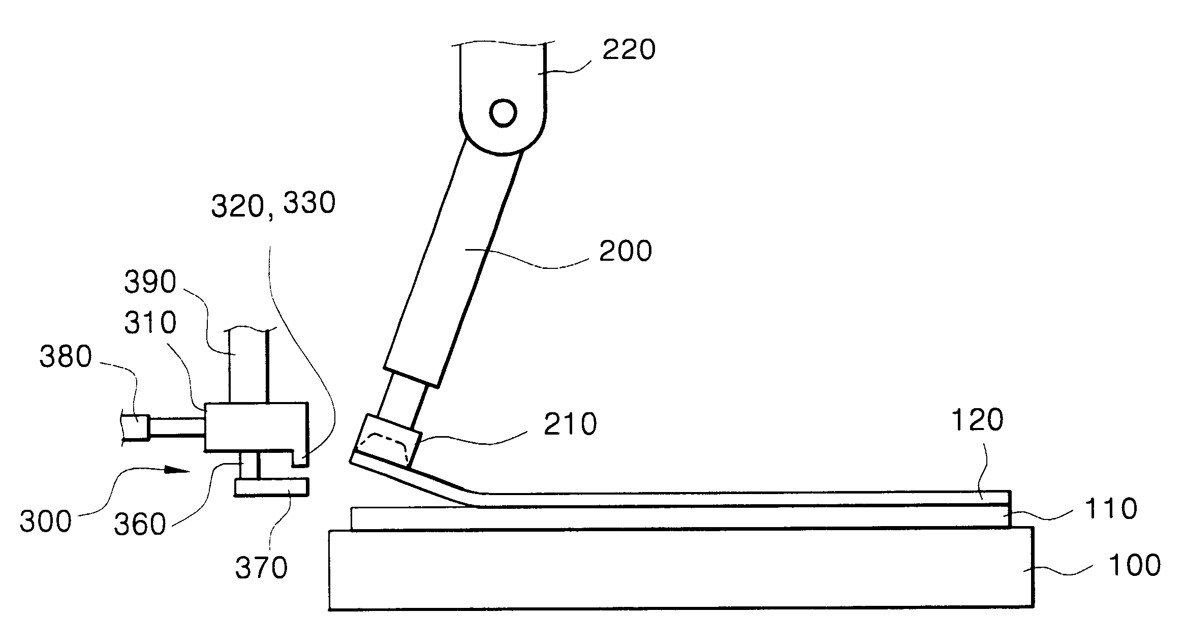
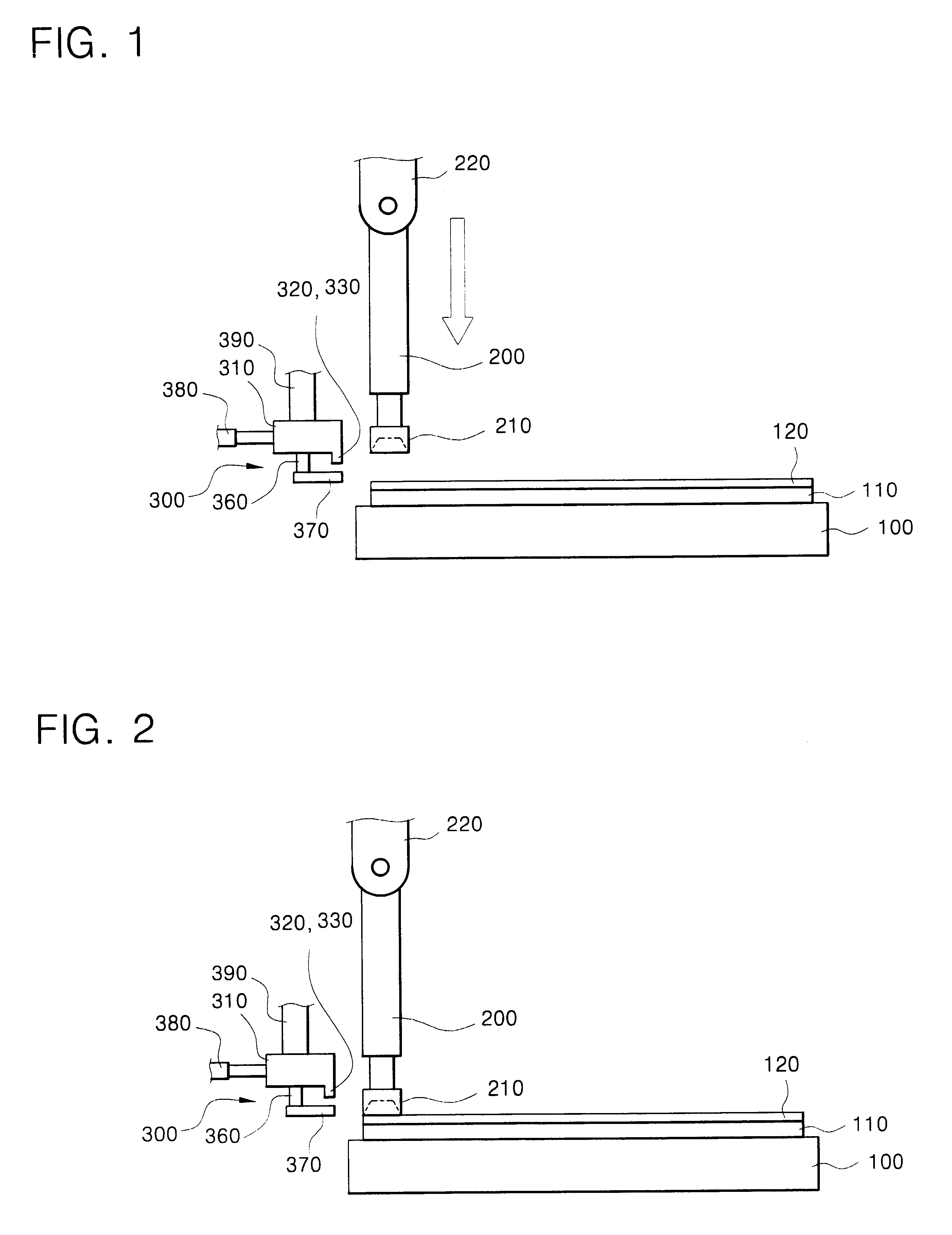
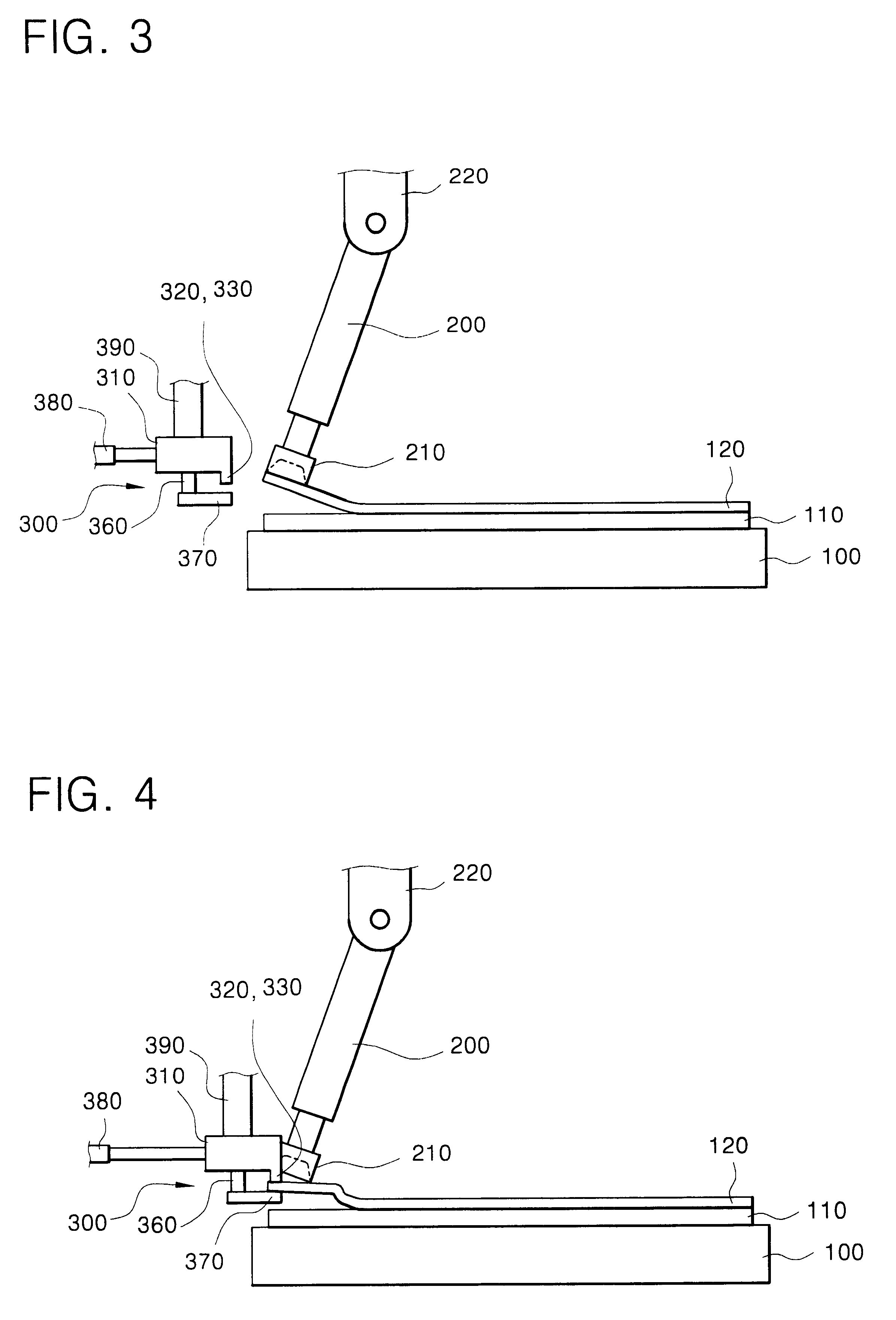
Protective film separator in semiconductor wafer grinding process
a technology of protective film and semiconductor wafer, which is applied in the direction of grinding machines, manufacturing tools, lapping machines, etc., can solve the problems of adversely affecting the final yield of the final wafer, increasing the expense of raw materials, and severe stress on the wafer surfa
- Summary
- Abstract
- Description
- Claims
- Application Information
AI Technical Summary
Benefits of technology
Problems solved by technology
Method used
Image

Examples
Embodiment Construction
Korean Patent Application No. 2001-2681, filed on Jan. 17, 2001, and entitled: "Protective Film Separator in Semiconductor Wafer Grinding Process", is incorporated by reference herein in its entirety.
The present invention now will be described more fully with reference to the accompanying drawings, in which preferred embodiments of the invention are shown. This invention may, however, be embodied in many different forms and should not be construed as being limited to the embodiments set forth herein; rather, these embodiments are provided so that this disclosure will be thorough and complete, and will fully convey the concept of the invention to those of ordinary skill in the art.
In general, a semiconductor process includes a single crystal silicon growing process, a device design process, a fabrication FAB process, an assembly process, and an inspection process. The single crystal silicon growing process produces a single crystal silicon ingot with a high purity and slices the sing...
PUM
| Property | Measurement | Unit |
|---|---|---|
| angle | aaaaa | aaaaa |
| adsorption | aaaaa | aaaaa |
| distance | aaaaa | aaaaa |
Abstract
Description
Claims
Application Information