Method and apparatus for testing IC device

a technology of electrical properties and ic devices, applied in semiconductor/solid-state device testing/measurement, instruments, de-stacking articles, etc., can solve the problems of difficult to test a large number of ic devices in a speedy and efficient manner, and the test time could become extremely long

Inactive Publication Date: 2003-02-04
HITACHI ELECTRONICS ENG CO LTD
View PDF13 Cites 106 Cited by
  • Summary
  • Abstract
  • Description
  • Claims
  • Application Information

AI Technical Summary

Problems solved by technology

In such a case, however, you cannot be sure if you can succeed in a data write-in test by one write-in action.
As a consequence, the testing time could become extremely long, making it difficult to test a large number of IC devices in speedy and efficient manner.
These irregularities in testing time among the respective test boards greatly affect the progress of operations in other stages, i.e., the operations in the IC device loading, unloading and preheating stages.

Method used


Image

  • Method and apparatus for testing IC device
  • Method and apparatus for testing IC device
  • Method and apparatus for testing IC device

Examples


Embodiment Construction

Hereafter, the present invention is described more particularly by way of its preferred embodiments. In the following description, the present invention is applied to testing of packaged IC devices under preheated or cooled conditions. However, it is to b e understood that the invention can be similarly applied to tests of similar IC devices at normal temperature.

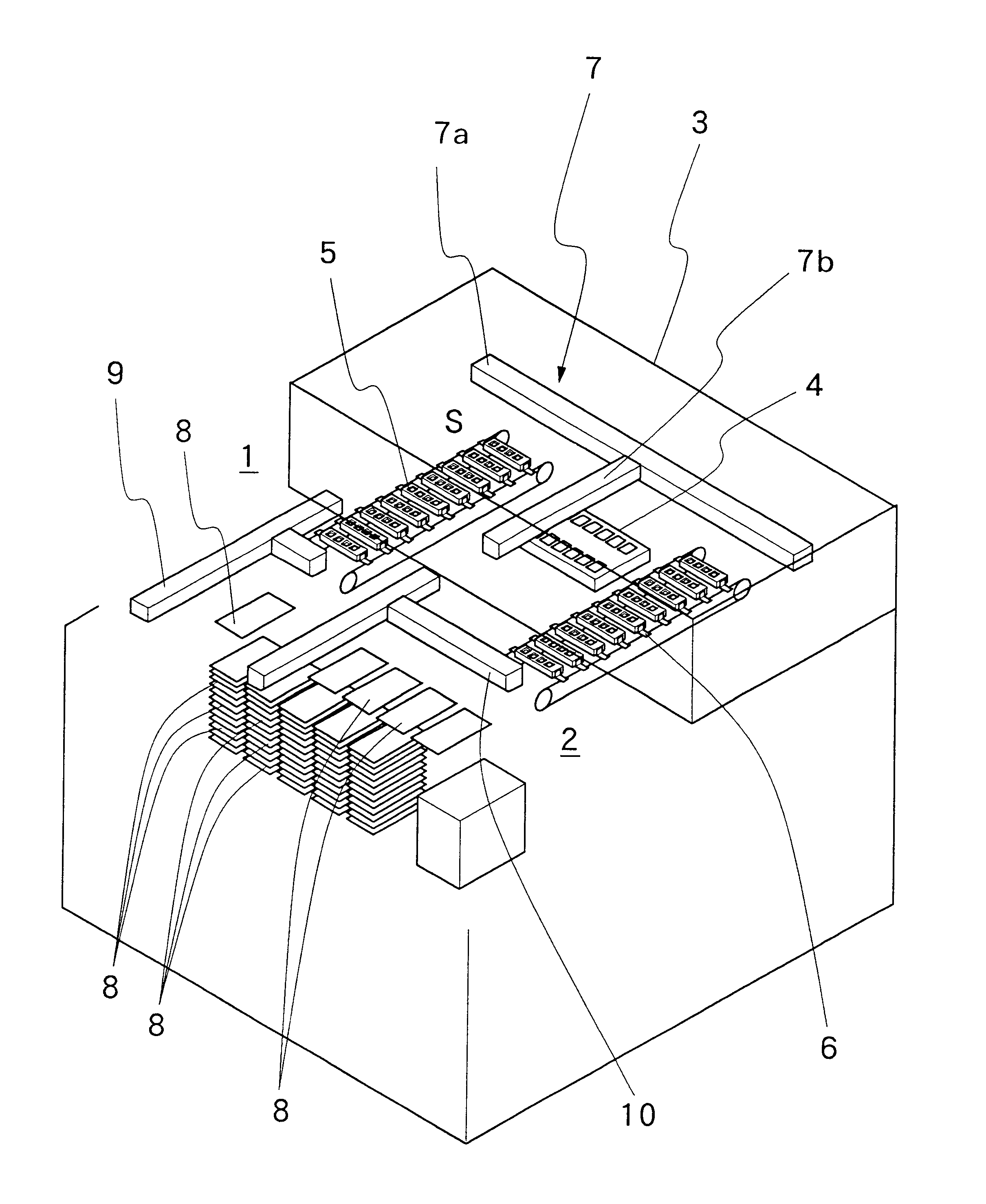
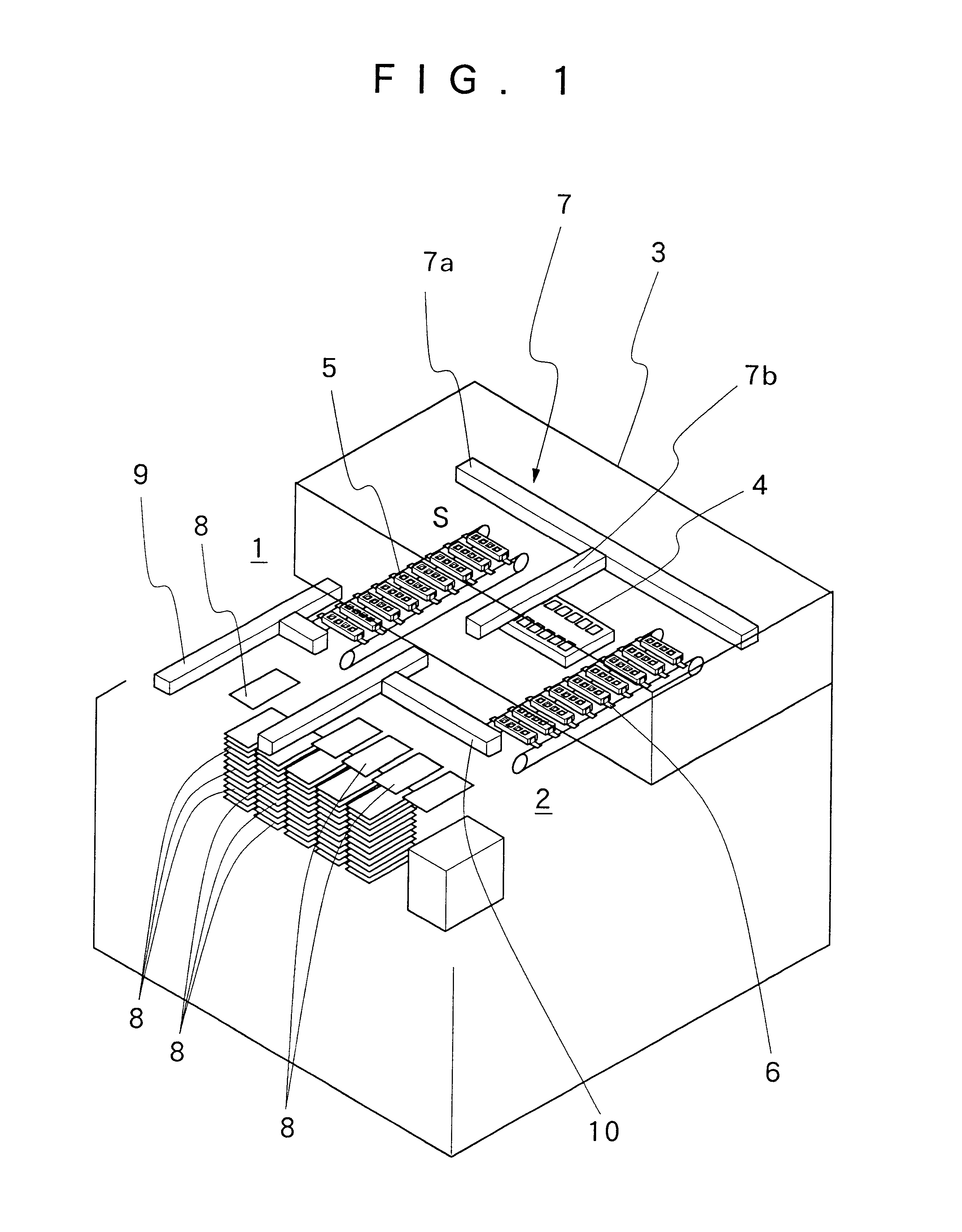
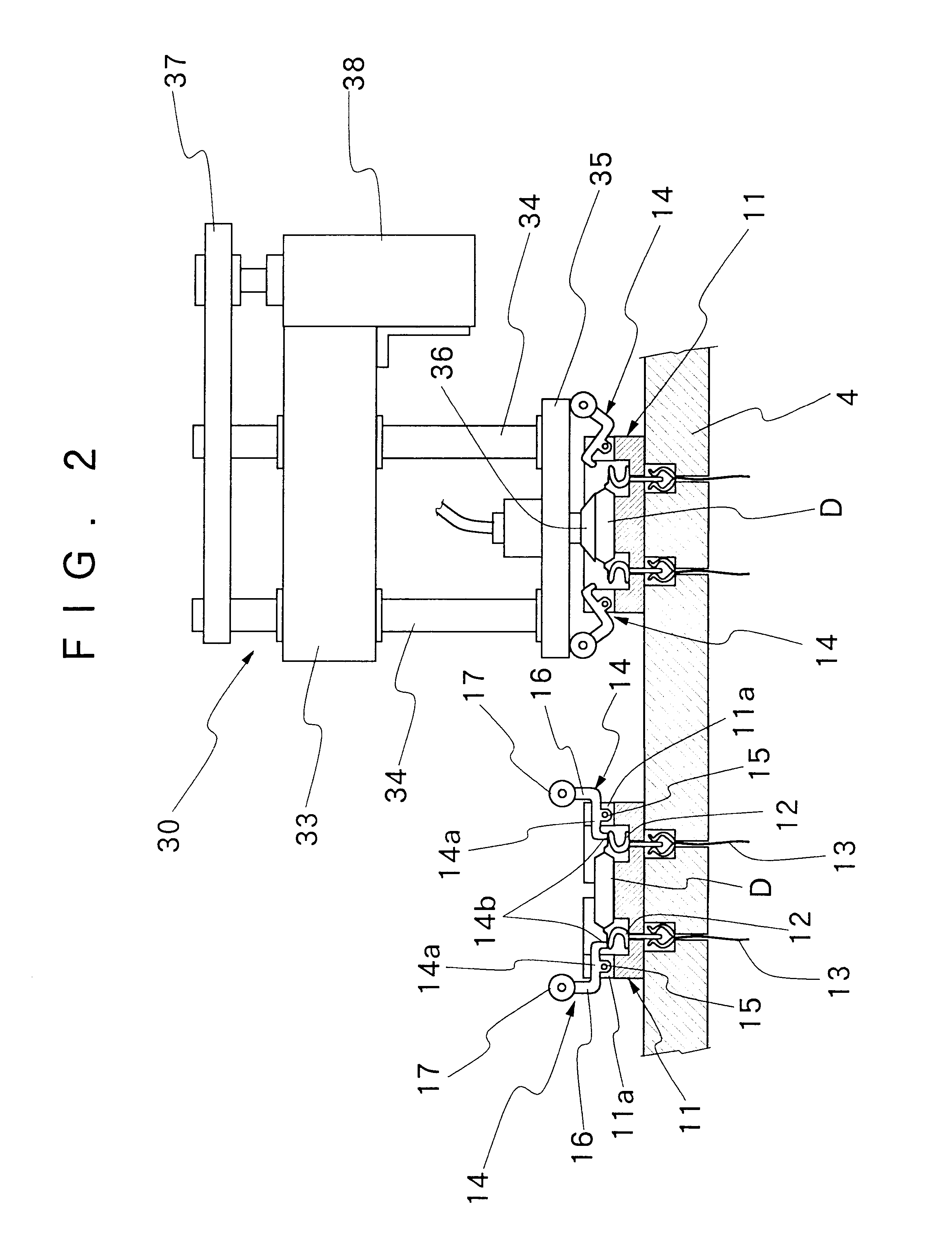
Shown in FIG. 1 is the general layout of an IC device testing apparatus according to the present invention, while shown in FIG. 2 is the construction of a test board having a number of packaged IC devices mounted thereon for a test of electrical properties. In these figures, indicated at 1 is a loader section or loading station, at 2 an unloader section or loading station and at 3 a thermostatic chamber. Provided within the thermostatic chamber 3 are a testing station with a test board 4, an inward IC feed conveyer 5 and an outward IC discharging conveyer 6. Further, an in-chamber transfer robot 7 is provided in the thermos...


PUM


Abstract

For testing electrical properties of packaged IC devices, there is provided an apparatus which includes a test board which is located at a testing station and provided with a plural number of contacting sockets for connecting individual IC devices to an IC tester separately and independently of each other, a loader which is located at a loading station and adapted to feed untested IC devices toward the test board, an unloader which is located at an unloading station and adapted to discharge tested IC devices from the test board at the testing station, and a device transfer mechanism which is movable across the testing station to transfer untested IC devices from the loader to the test board and also to transfer tested IC devices from the test board to the unloader. Upon detecting completion of a test on one of IC devices in one socket of the test board, a fresh untested IC device is transferred to the testing station to replace the tested IC device. As soon as the fresh IC device is set in position in that socket, execution of a test program is started with respect to that socket on the test board.

Description

1. Field of the ArtThis invention relates to a method and an apparatus for testing electrical properties of IC devices, particularly suitable for use in testing packaged IC devices such as, for example, EEPROM (Electrically Erasable Programmable ROM) and the like.2. Prior ArtGenerally, apparatus which are in use for testing electrical properties of packaged IC devices are largely constituted by an IC tester and an IC handler. An IC tester is arranged to check for defects of IC devices by measuring electrical properties of connected IC devices according to predetermined test patterns. On the other hand, an IC handler is arranged to electrically connect respective IC devices to the IC tester, and to classify tested IC devices according to test results.Accordingly, the IC handler which is generally employed for connecting and disconnecting IC devices to and from the IC the IC tester is largely constituted by a test board for removably mounting IC devices thereon, a loader for feeding I...

Claims


Application Information

Patent Timeline
Patent Type & Authority Patents(United States)
IPC IPC(8): B65G57/04B65G59/02B65G57/02G01R31/26H01L21/66
CPCB65G57/04G01R31/2893B65G59/02H01L22/00
Inventor SUZUKI, TETSUYAOKITSU, AKIRA
Owner HITACHI ELECTRONICS ENG CO LTD
Why Eureka
Try Eureka