Method for timing analysis during automatic scheduling of operations in the high-level synthesis of digital systems

a technology of automatic scheduling and digital systems, applied in the field of electronic design automation, can solve the problems of multiplexing cost, unable to move/rescheduled output operations, and upset the block-to-block communication protocol

Inactive Publication Date: 2003-02-04
CADENCE DESIGN SYST INC
View PDF13 Cites 8 Cited by
  • Summary
  • Abstract
  • Description
  • Claims
  • Application Information

AI Technical Summary

Benefits of technology

Briefly, a design-timing-determination method embodiment of the present invention for an electronic design automation system approximates the timing of a whole design quickly and on-the-fly. Such allows a scheduling system to construct operation schedules that are ultimately realizable. A timing analysis is applied each time an individual operation is scheduled, and may be called many times to get a single operation scheduled. A graph representing combinational logic is partitioned into a collection of logic trees with nodes that represent gates and terminals, and arcs that represent connections. A compacted model of each logic tree is constructed by replacing them with equivalent trees having no interior nodes. The timing of the original circuit is analyze

Problems solved by technology

These input/output operations cannot be moved, or rescheduled, from one state to another, because to do so would probably upset the block-to-block communication protocol.
But complications can arise when more than one hardware resource of a given bit-width and function is needed.
Considerations include multiplexing cost, the creation of false timing paths, register assignment, and even using a large resources for small operations.
Calculating a minimum set of resources for an entire process is difficult but rewarding.
But register and storage allocations can be complicated if data values can form mutually exclusive sets or can share storage.
Th

Method used


Image

  • Method for timing analysis during automatic scheduling of operations in the high-level synthesis of digital systems
  • Method for timing analysis during automatic scheduling of operations in the high-level synthesis of digital systems
  • Method for timing analysis during automatic scheduling of operations in the high-level synthesis of digital systems

Examples


Embodiment Construction

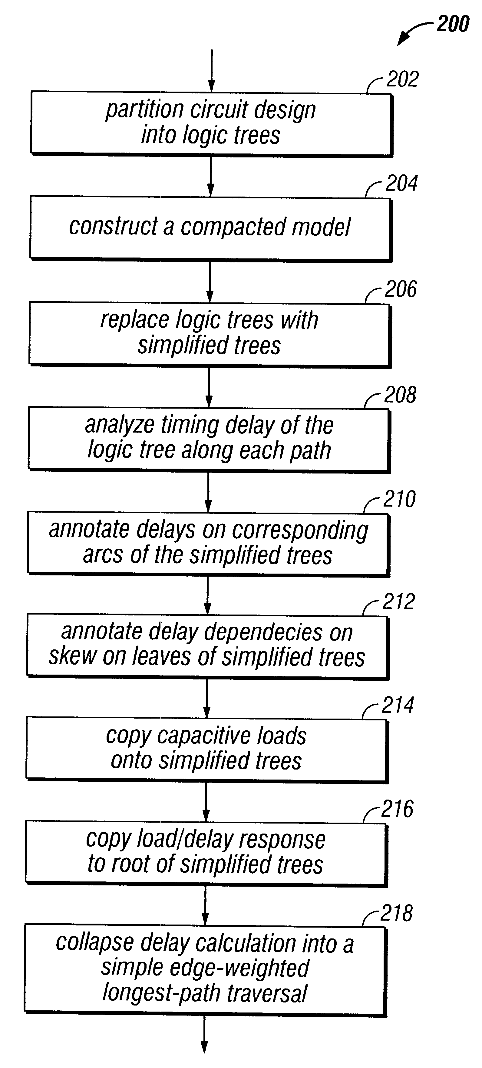
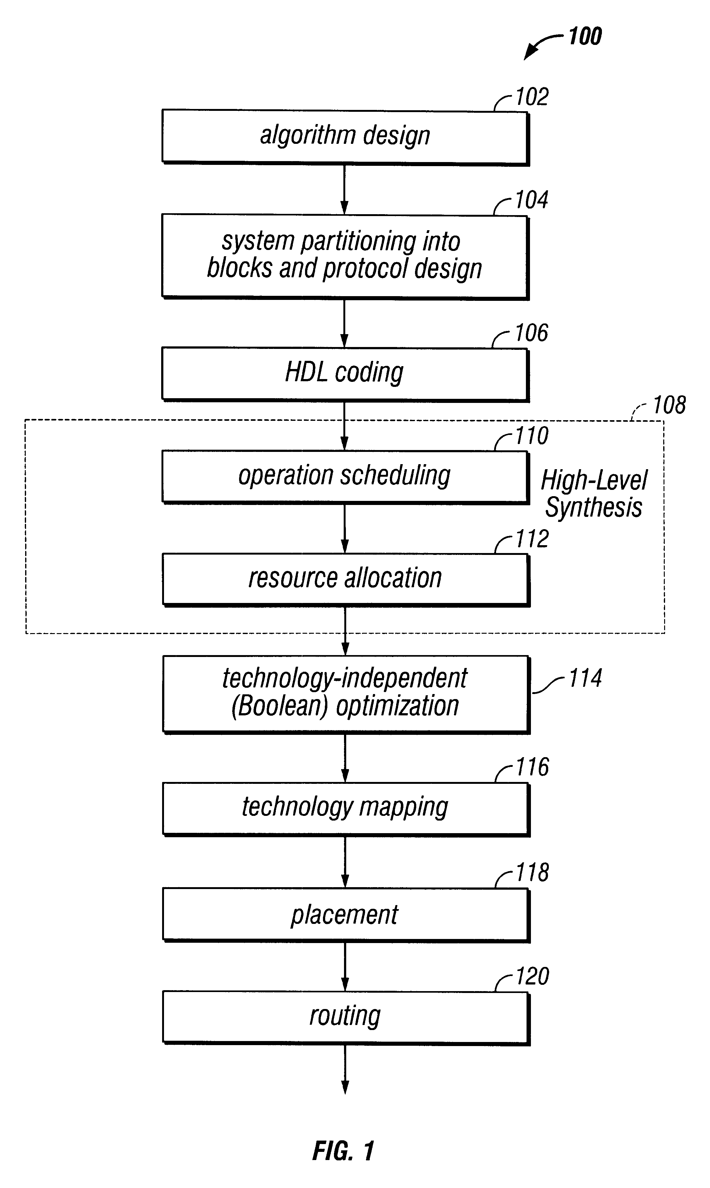
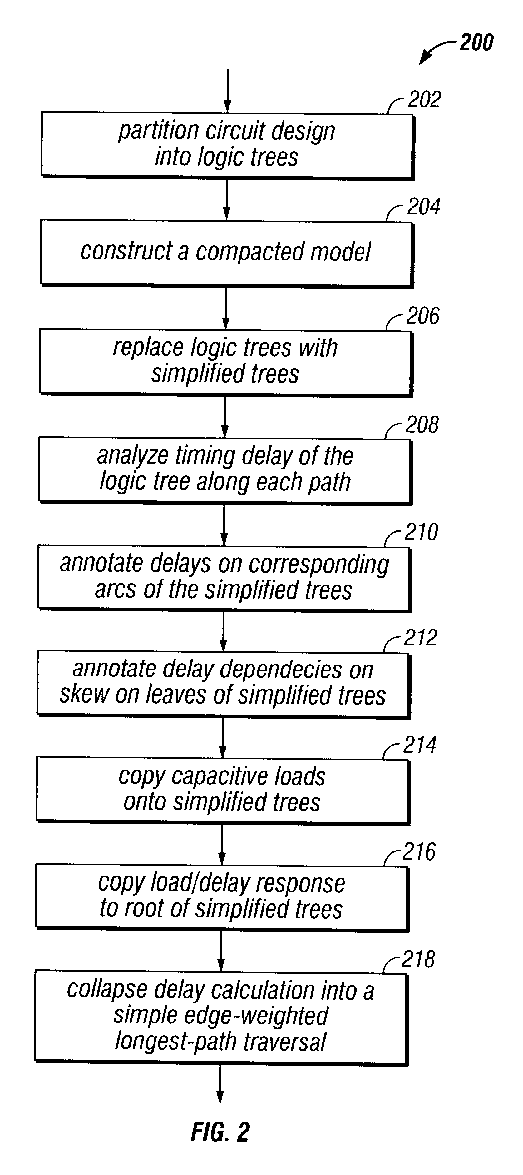
FIG. 1 represents an electronic design automation (EDA) method embodiment of the present invention, and is referred to herein by the general reference numeral 100. The EDA method begins with an algorithm design step 102. The system design is partitioned into blocks and protocol design in a step 104. Verilog or other kind of hardware description language (HDL) coding is done in a step 106. A high-level synthesis (HLS) step 108 includes an operation scheduling step 110 and a resource allocation step 112. A timing analysis is applied each time an individual operation is scheduled, and may be called many times to get a single operation scheduled. A technology-independent (Boolean) optimization step 114 follows. A technology mapping step 116 maps the abstract Boolean gates of the circuit to standard cells from a technology library, for example. A placement step 118 locates the gates on the chip real estate, and a routing step 120 interconnects them with wires.

The timing analysis starts w...


PUM


Abstract

A design-timing-determination process for an electronic design automation system approximates the timing of a whole design quickly and on-the-fly. Such allows a scheduling system to construct operation schedules that are ultimately realizable. A timing analysis is applied each time an individual operation is scheduled, and may be called many times to get a single operation scheduled. A graph representing combinational logic is partitioned into a collection of logic trees with nodes that represent gates and terminals, and arcs that represent connections. A compacted model of each logic tree is constructed by replacing them with equivalent trees having no interior nodes. The timing of the original circuit is analyzed along each path from the leaves to the roots. A propagation delay for each path is determined, and such is annotated onto each corresponding arc of the simplified tree. Any dependency of the propagation delay in the original circuit on the slew rate of their input signals is annotated onto the corresponding leaf of the simplified tree. Capacitive loads can also be copied from the logic-tree leaves and annotated on the simplified-tree leaves. Any load/delay response curves of the output gate at the apex of the logic tree and is copied to the root of the simplified tree. The entire delay calculation is collapsed into a simple edge-weighted longest-path traversal, and is much simpler than trying to compute the slew rates and delays for each cell in a circuit.

Description

BACKGROUND OF THE PRESENT INVENTION1. Technical FieldThe present invention relates to electronic design automation and more particularly to timing analysis during automatic scheduling of operations in the high-level synthesis of digital systems.2. Description of the Prior ArtHigh-level synthesis (HLS) automates certain subtasks of a digital system design in an electronic design automation (EDA) system. A system architect begins by designing and validating an overall algorithm to be implemented, e.g., using C, C++, a specialized language, or a capture system. The resulting architectural specification is partitioned into boards, chips, and blocks. Each block is a single process having its own control flow. There are usually tens to hundreds of such blocks in a modem large-scale chip design. Typical blocks represent whole filters, queues, pipeline stages, etc. Once a chip has been partitioned into its constituent blocks, any needed communication protocols have to be constructed. Such p...

Claims


Application Information

Patent Timeline
IPC IPC(8): G06F17/50
CPCG06F17/505G06F17/5045G06F30/327G06F30/30G06F2119/12G06F30/3312
Inventor KNAPP, DAVID
Owner CADENCE DESIGN SYST INC
Why Eureka
Try Eureka