Substrate processing system and substrate processing method

a processing system and substrate technology, applied in the field of substrate processing system and substrate processing method, can solve the problems of remarkably decreasing the system throughput, unable to know when one lot is processed, and tending to confuse which cassette contains processed wafers

Inactive Publication Date: 2003-02-25
TOKYO ELECTRON LTD
View PDF13 Cites 65 Cited by
  • Summary
  • Abstract
  • Description
  • Claims
  • Application Information

AI Technical Summary

Benefits of technology

The calculation processing portion preferably has a storing portion. The calculation processing portion calculates the process completion prediction time corresponding to old process procedures and completion times thereof stored in the storing portion. Thus, the calculation processing portion can properly calculate the process completion prediction time.
The calculation processing portion preferably calculates a cassette changeable time period for which a cassette that contains unprocessed substrates can be changed corresponding to the second process completion prediction time. Thus, since as information that is more detail than the process completion prediction time, a time at which a cassette that contains unprocessed substrates can be obtained. Thus, the operator can more effectively change a cassette that contains unprocessed substrates. Alternatively, the calculation processing portion calculates the cassette changeable time period for which a processed wafer cassette CR can be changed corresponding to the first and third process completion prediction times. Thus, as information that is more detail than the process completion prediction time, a time at which a cassette that contains processed wafers can be obtained. Thus, the operator can more effectively change a cassette that contains processed cassettes.

Problems solved by technology

However, when the operator repeats such an operation, he or she tends to confuse which cassette contains processed wafers.
In addition, the operator cannot know when one lot is processed.
If the operator forgets to change cassettes, the system does not properly operates, thereby remarkably decreasing the throughput of the system.

Method used


Image

  • Substrate processing system and substrate processing method
  • Substrate processing system and substrate processing method
  • Substrate processing system and substrate processing method

Examples


first embodiment

(First Embodiment)

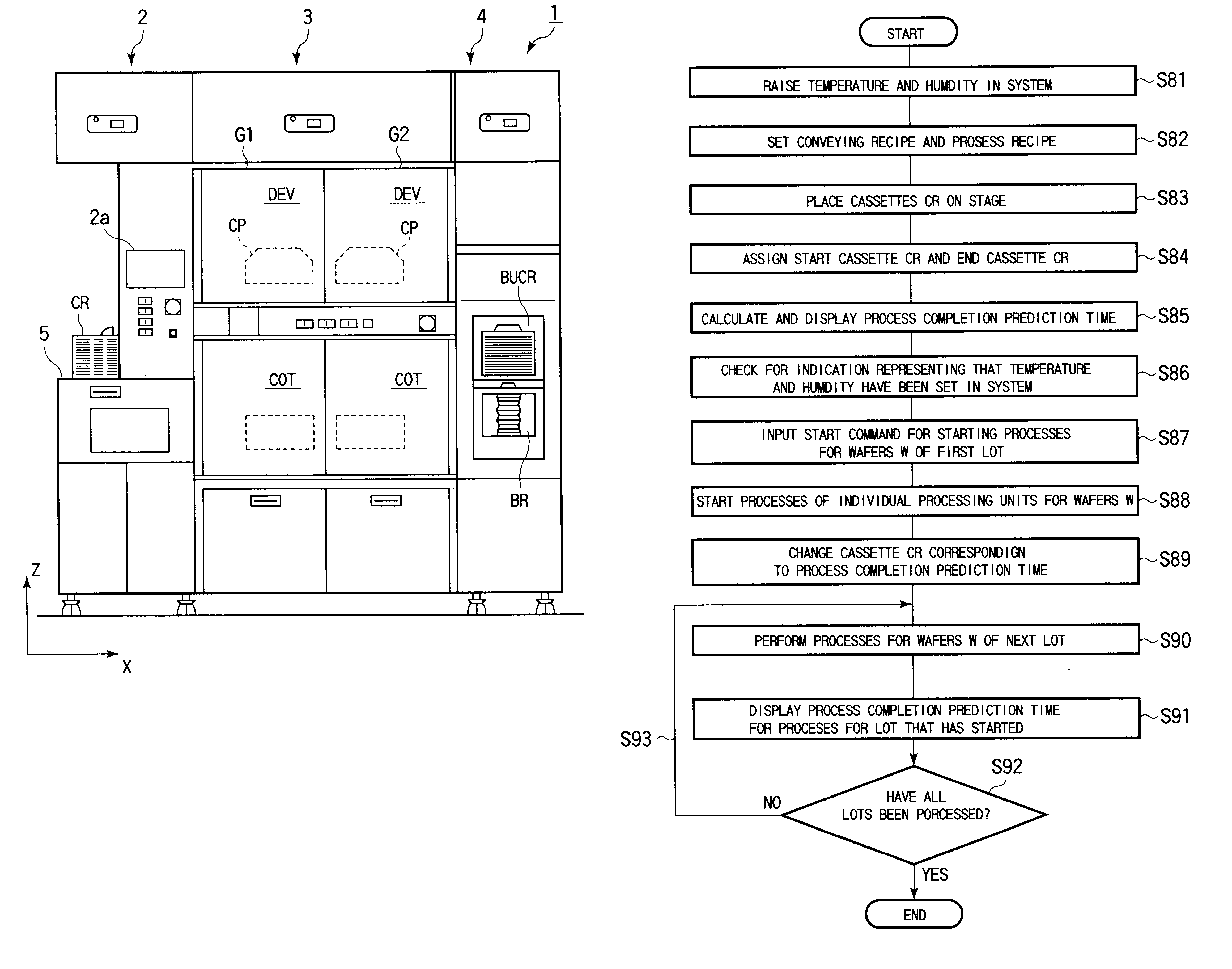
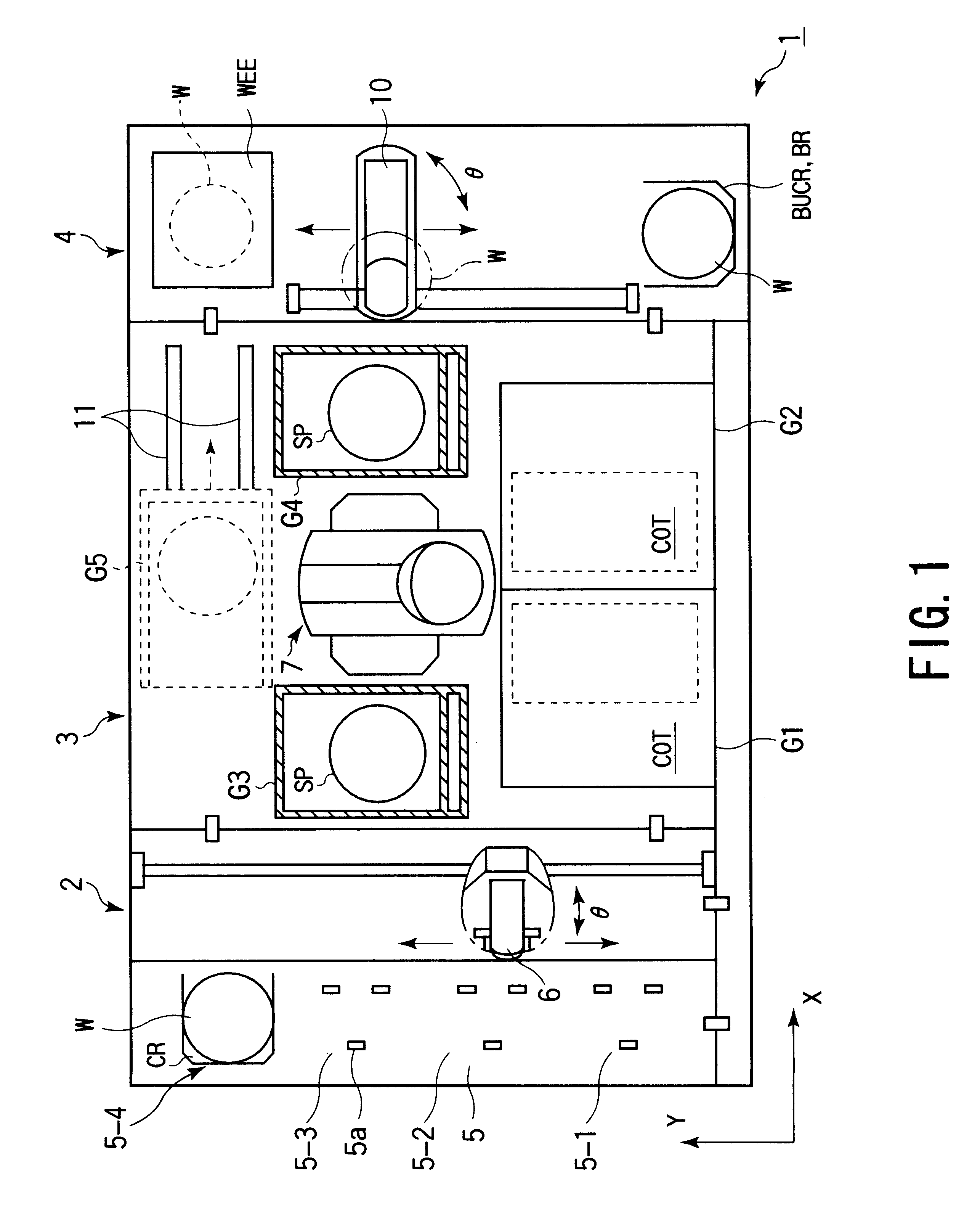
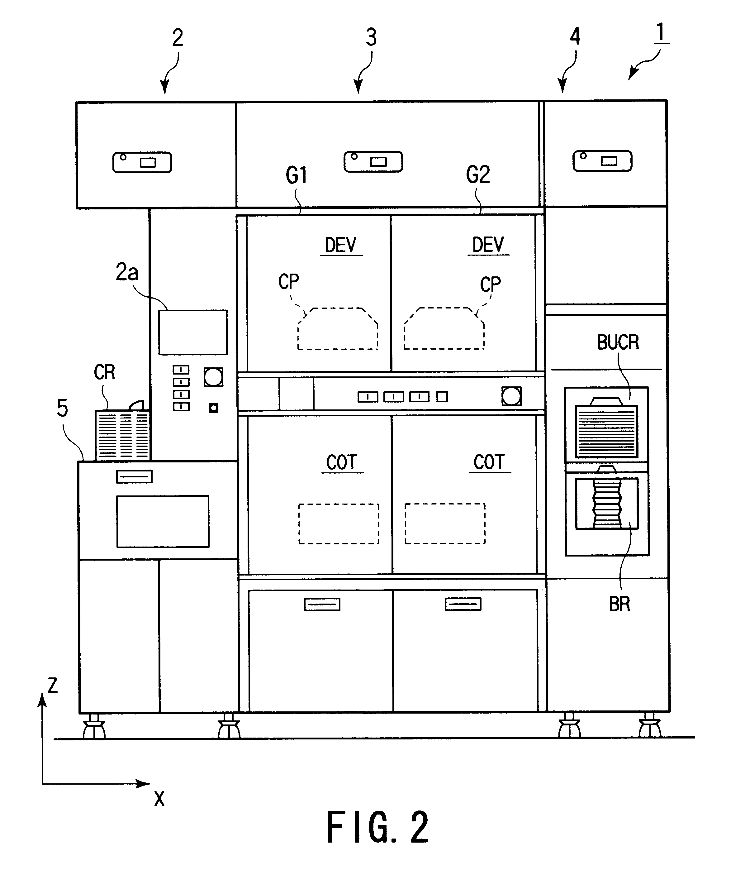
FIGS. 1 to 3 are schematic diagrams showing the overall structure of a substrate processing system 1 according to the present invention. The substrate processing system 1 comprises a loading / unloading portion 2, a processing portion 3, and an interface portion 4. The loading / unloading portion 2 successively extracts wafers W from a cassette CR. The processing portion 3 performs a resist solution coating process and a developing process for a wafer W extracted from the loading / unloading portion 2. The interface portion 4 transfers the wafer W that has been coated with a resist solution to an exposing device 12. The interface portion 4 has a second sub-arm mechanism 10. The second sub-arm mechanism 10 exchanges the wafer W with the exposing device 12. The loading / unloading portion 2 has a holding table 5 on which a semiconductor wafer W is extracted and returned from / to a cassette CR.

As shown in FIG. 1, in the loading / unloading portion 2, a plurality of (for example,...

second embodiment

(Second Embodiment)

Next, a modification of the first embodiment will be described as a second embodiment of the present invention. According to the second embodiment, when the operator could not change a cassette CR in a cassette changeable time period, it is compensated.

As was described in the first embodiment, the cassette changeable time period has been obtained when real processes for one of a plurality of lots are started. However, when the operator could not mistakenly change a cassette CR in the cassette changeable time period, it deviates from the real process start time for the first lot. In other words, since a cassette CR has not been changed, the continuous processes are not started. However, since the cassette changeable time period elapses, the operator may be informed of an incorrect cassette changeable time period.

To solve such a problem, according to the second embodiment of the present invention, the controller 59 cumulates time lags corresponding to sensor outputs...


PUM

PropertyMeasurementUnit
process completion prediction timeaaaaaaaaaa
timeaaaaaaaaaa
time periodaaaaaaaaaa

Abstract

The present invention is a substrate processing method comprising the steps of successively extracting unprocessed wafers from a cassette, successively conveying the extracted wafers to a plurality of processing units, causing the processing units to process the wafers in parallel, and returning the processed wafers to a cassette. A process completion prediction time at which processes for one lot are completed is calculated and displayed corresponding to a process recipe that has been set to a plurality of wafers for at least one lot. Corresponding to the process completion prediction time, a cassette that contains a plurality of unprocessed wafers for one lot is accepted. A cassette that contains a plurality of processed wafers for one lot is returned.

Description

1. Field of the InventionThe present invention relates to a substrate processing system and a substrate processing method for performing a sequence of processes for various types of substrates such as semiconductor wafers and liquid crystal display (LCD) glass substrates.2. Description of the Related ArtIn fabrication processes for LCD substrates and semiconductor devices, fine circuit patterns are formed using a photolithography technology. In the photolithography technology, a resist is coated in a film shape on the front surface of a raw substrate such as an LCD substrate or a semiconductor wafer and then exposed with a predetermined pattern. After the exposed pattern is developed and etched, a desired circuit pattern is obtained.Recently, as the sizes of semiconductor wafers are becoming large, in the photolithography process, wafers are successively processed. For example, in a complex processing system that performs both of a resist coating process and a developing process, wa...

Claims


Application Information

Patent Timeline
Patent Type & Authority Patents(United States)
IPC IPC(8): G03F7/20H01L21/00B65G49/06B65G49/07G05B19/418H01L21/02H01L21/027H01L21/677
CPCG03F7/7075G05B19/41865H01L21/67248Y10S414/14G05B2219/31429Y02P90/02H01L21/02
Inventor TATEYAMA, MASANORIFUJIMARU, SYUZO
Owner TOKYO ELECTRON LTD
Why Eureka
Try Eureka