Method and apparatus for reducing signal timing skew on a printed circuit board

a technology of printed circuit boards and signal timing skew, which is applied in the direction of generating/distributing signals, removing conductive materials by irradiation, instruments, etc., and can solve the problems of imposing additional manufacturing limitations, high cost, and relatively high implementation cos

Inactive Publication Date: 2003-02-25
MICRON TECH INC
View PDF7 Cites 63 Cited by
  • Summary
  • Abstract
  • Description
  • Claims
  • Application Information

AI Technical Summary

Problems solved by technology

Many techniques have been proposed, but all involve substantial costs, as well as imposing additional manufacturing limitations.
The conduction pattern has to be carefully designed and conditioned and is therefore relatively expensive to implement.
Moreover, the conducti

Method used


Image

  • Method and apparatus for reducing signal timing skew on a printed circuit board
  • Method and apparatus for reducing signal timing skew on a printed circuit board
  • Method and apparatus for reducing signal timing skew on a printed circuit board

Examples


Embodiment Construction

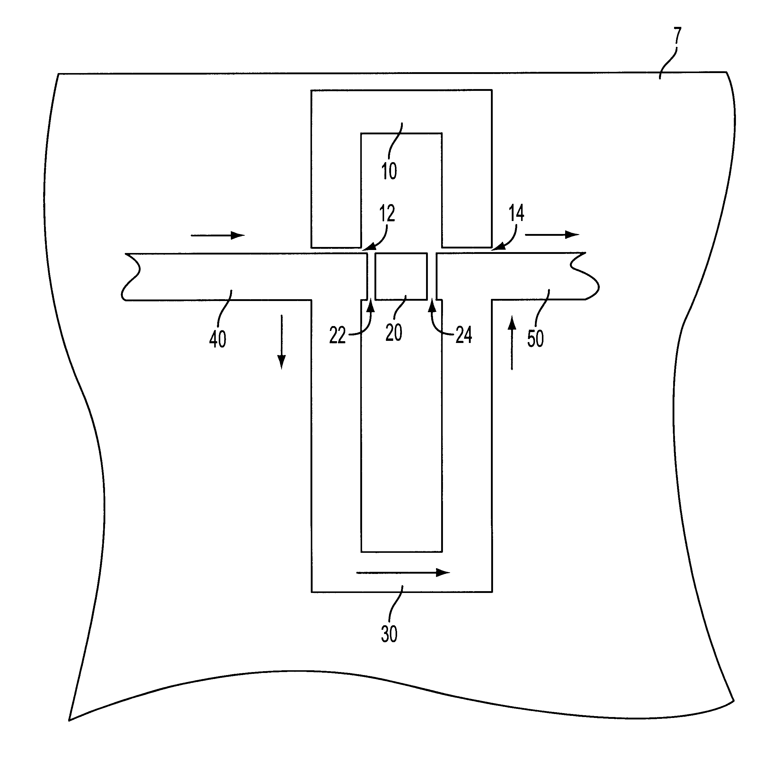
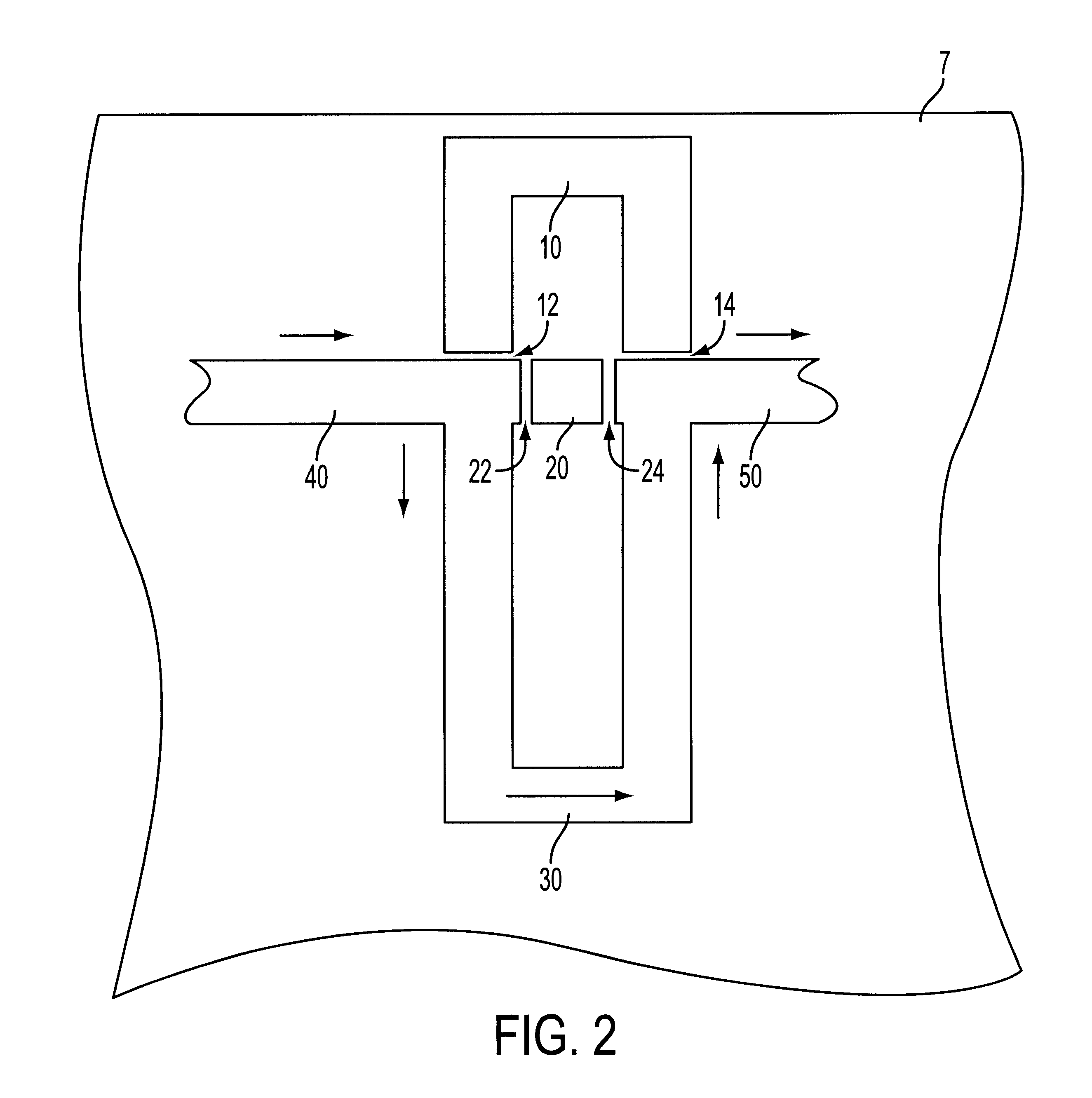
FIG. 7 illustrates three memory modules, each containing a plurality of memory chips on a printed circuit board, which were serially interconnected to demonstrate use of the invention. The three memory modules 50, 60, 70 have a series connected clock signal. Each untuned memory module 50, 60, 70 has an inherent clock signal-to-reference signal skew of 100 ps. Thus, the three untuned memory modules have a cumulative clock signal-to-reference signal skew of 300 ps. This number increases as the number of memory modules having serially connected clock signals increases. Each memory module also is provided with a respective signal path adjustment section 55, 65, 75 corresponding to one of the embodiments shown in FIGS. 1, 2, 4, 5, or 6 at the output side thereof. The clock signals connect from the output of one memory module, i.e., module 50, to the input of another memory module, i.e., module 60.

To adjust the clock timing skew, the adjustment section 55, 65, 75 of each memory module 50,...


PUM


Abstract

An apparatus and method are described for reducing the timing skew on a printed circuit board including a plurality of conductive traces interconnecting a first node and a second node. At least one section is removed from at least one printed circuit board trace to thereby sever a trace and prevent signals passing from the first node to the second node from following the severed trace. In this manner, signal path length can be adjusted to reduce timing skews in the circuit. Sections are removed from the traces by using a laser, CVD, a router, a plasma or by passing sufficient current through weakened areas of the traces.

Description

1. Field of the InventionThe present invention relates to a method and apparatus for reducing skew of signals passing through a memory module. More specifically, the present invention relates to a method and apparatus for reducing the timing skew by adjusting the length of the signal traces on a printed circuit board of the memory module.2. Description of the Related ArtIt is desirable to attempt to eliminate timing skew between signals propagating through high speed memory modules and other types of high speed integrated circuit ("IC") modules or circuits. Many techniques have been proposed, but all involve substantial costs, as well as imposing additional manufacturing limitations.U.S. Pat. No. 5,260,892, for example, describes a method and apparatus for manufacturing an improved Dynamic Random Access Memory ("DRAM") electrical signal interconnect structure having special application to Single In-line Memory Modules ("SIMMs"). The structure contains an on-board buffer for deriving...

Claims


Application Information

Patent Timeline
IPC IPC(8): G06F1/10H05K1/00H05K1/02H05K3/02
CPCG06F1/10H05K1/0248H05K1/0293H05K3/027H05K2201/09263H05K2201/0969H05K2203/175H05K2201/0979H05K2203/095H05K2203/107H05K2203/1115H05K2203/1338H05K2203/171H05K2201/09736
Inventor CUTHBERT, DAVID
Owner MICRON TECH INC
Why Eureka
Try Eureka