Lateral conduction Schottky diode with plural mesas

a lateral conduction and schottky diode technology, applied in the field of schottky diode structures and assemblies, can solve the problems of high series resistance, low carrier mobility of silicon-based schottky diodes, and relatively narrow band gaps

Active Publication Date: 2006-08-01
POWER INTEGRATIONS INC
View PDF25 Cites 90 Cited by
  • Summary
  • Abstract
  • Description
  • Claims
  • Application Information

AI Technical Summary

Benefits of technology

[0047]The flip chip arrangements of the invention have the added advantage that when a thermally conductive submount material is used, such as silicon, aluminum nitride (AlN) or an electrically isolated metal, the submount also transports heat from the Schottky diode, thereby alleviating heat buildup at the thermally insulating substrate of the Schottky diode.

Problems solved by technology

Silicon-based Schottky diodes have the disadvantage, however, that silicon has a low carrier mobility and a relatively narrow band gap.
Further, for higher voltage applications, a thick, low doped base must be used which leads to higher series resistance, a greater forward voltage drop, and increased heat dissipation, thereby making silicon-based Schottky diodes unsuitable for such applications.
Moreover, at higher temperatures, the reverse leakage current increases dramatically and negates the rectification properties of the device.
Devices having a lateral conduction path, however, are prone to high on-resistances when the device is forward-biased because the forward current must travel over a relatively long conduction path determined by the horizontal dimensions of the device.
Moreover, because the forward current flows laterally from the Schottky metallic contact to the ohmic metallic contact, current flow away from the Schottky metallic contact is often non-uniformly distributed so that the current density is crowded along the edge of the contact.
The electrically insulating substrate of the lateral conducting Schottky diode is also typically a poorer thermal conductor and thus dissipates heat less efficiently than vertical devices.
The poorer heat dissipation increases the complexity of the device packaging because alternative ways of heat removal must be employed.
Additionally, the device packaging is further complicated by the presence of both the Schottky metallic contact and the ohmic metallic contact on the same side of the laterally conducting device which requires more complex interconnections than those of vertically conducting devices in which the contacts are on opposite sides.

Method used


Image

  • Lateral conduction Schottky diode with plural mesas
  • Lateral conduction Schottky diode with plural mesas
  • Lateral conduction Schottky diode with plural mesas

Examples


Embodiment Construction

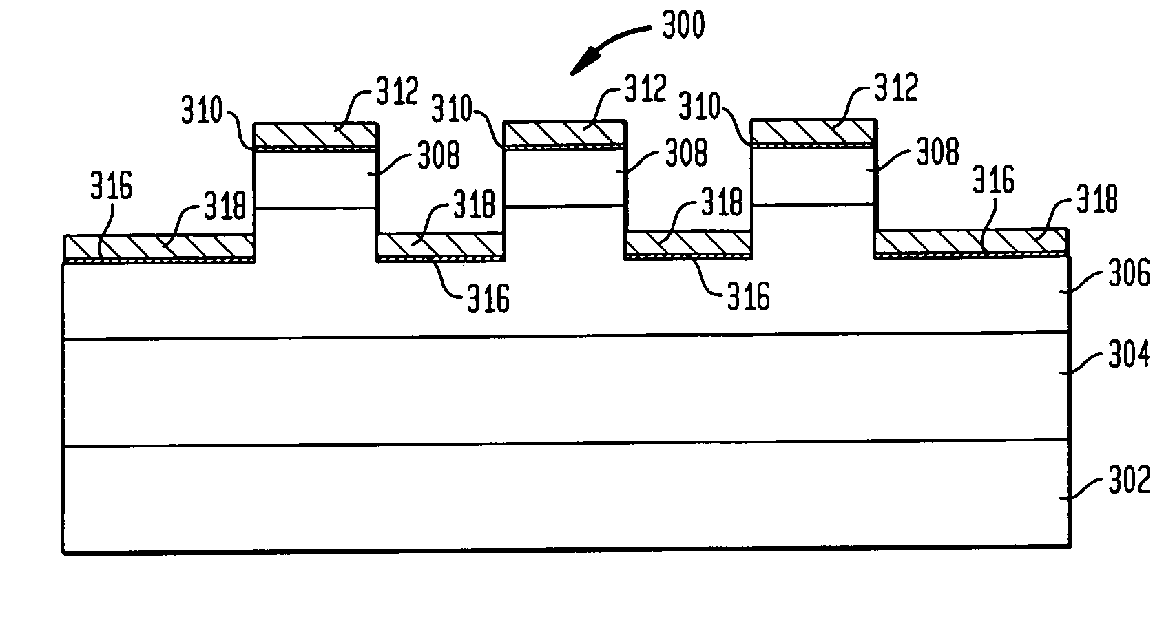
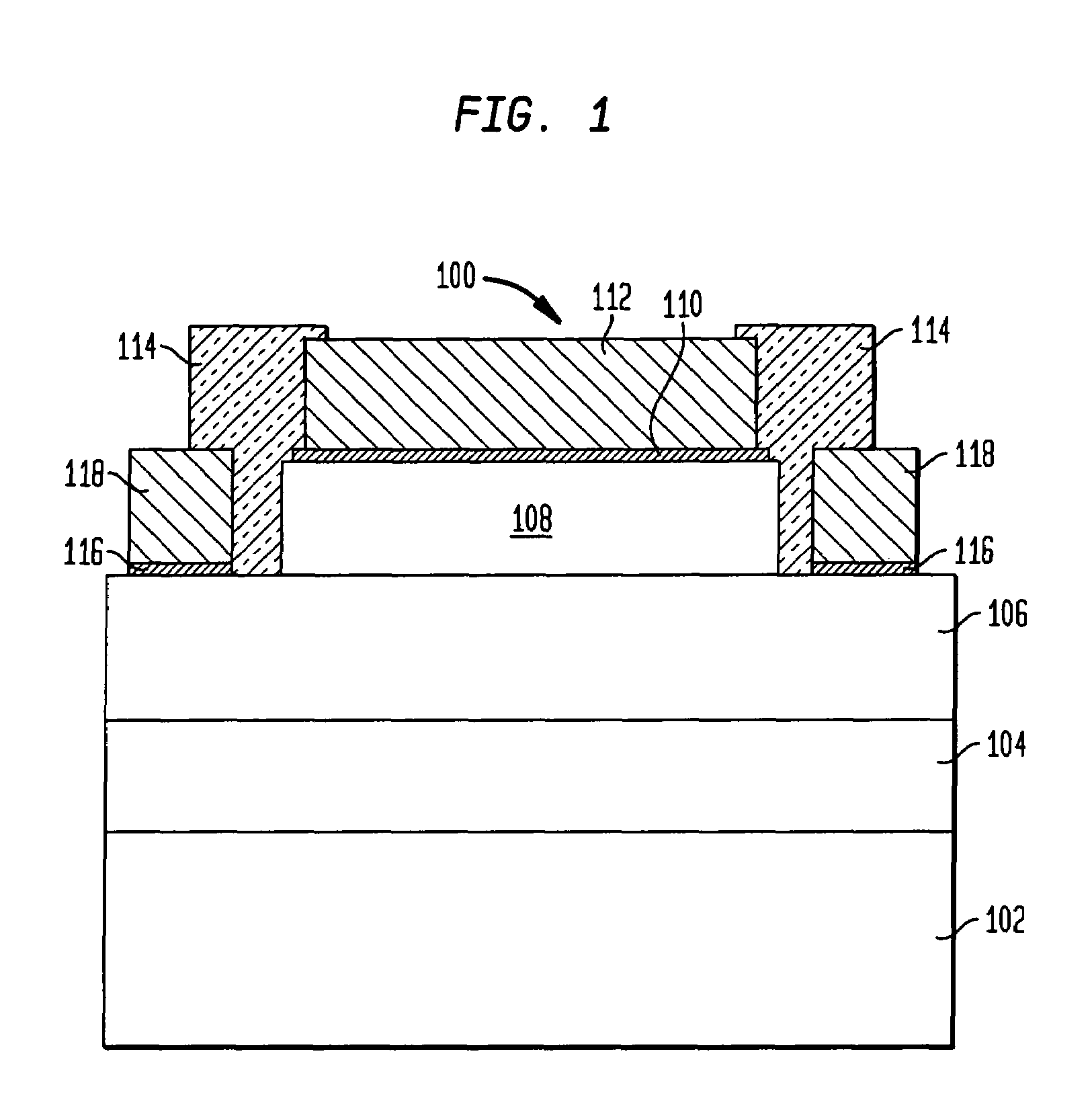
[0025]FIG. 1 illustrates a cross-sectional view of a known laterally conducting Schottky diode 100. The Schottky diode includes an electrically insulating substrate 102 that is typically a poor thermal conductor. A buffer layer 104 may be provided atop the substrate 102, and a highly doped semiconductor layer 106 is located atop the buffer layer 104 or, when the buffer layer is not present, directly atop the substrate 102. A lower doped semiconductor layer 108 is disposed atop a portion of the more highly doped semiconductor layer 106, and a Schottky metal contact 110 is located atop the lower doped semiconductor layer 108 and forms a metal-to-semiconductor junction with the lower doped layer. An ohmic metal contact is disposed atop the exposed portion of the highly doped layer 106. A thicker bond pad metal layer 112 is disposed atop the Schottky metal contact 110 and a further bond pad metal layer 118 is disposed atop the ohmic metal contact 116. A passivation layer 114 may be form...


PUM


Abstract

A lateral conduction Schottky diode includes multiple mesa regions upon which Schottky contacts are formed and which are at least separated by ohmic contacts to reduce the current path length and reduce current crowding in the Schottky contact, thereby reducing the forward resistance of a device. The multiple mesas may be isolated from one another and have sizes and shapes optimized for reducing the forward resistance. Alternatively, some of the mesas may be finger-shaped and intersect with a central mesa or a bridge mesa, and some or all of the ohmic contacts are interdigitated with the finger-shaped mesas. The dimensions of the finger-shaped mesas and the perimeter of the intersecting structure may be optimized to reduce the forward resistance. The Schottky diodes may be mounted to a submount in a flip chip arrangement that further reduces the forward voltage as well as improves power dissertation and reduces heat generation.

Description

BACKGROUND OF THE INVENTION[0001]The present invention is directed to semiconductor devices and, more particularly, to Schottky diode structures and assemblies.[0002]Schottky diodes are desired for applications where energy losses while switching from forward bias to reverse bias and back can significantly impact the efficiency of a system and where high current conduction is desired under forward bias and little or no conduction is desired under reverse bias, such as when used as an output rectifier in a switching power supply. The Schottky diodes have lower turn-on voltages because of the lower barrier height of the rectifying metal-to-semiconductor junction and have faster switching speeds because they are primarily majority carrier devices.[0003]Presently, most Schottky diodes are silicon-based, vertical conduction devices. In such devices, a Schottky metallic contact is formed on one surface of a silicon body, an ohmic metallic contact is formed on an opposite surface of the si...

Claims


Application Information

Patent Timeline
Patent Type & Authority Patents(United States)
IPC IPC(8): H01L29/47H01L21/60H01L29/06H01L29/20H01L29/872
CPCH01L24/81H01L29/0692H01L29/872H01L2924/12032H01L29/2003H01L2224/81801H01L2924/01012H01L2924/01013H01L2924/0103H01L2924/01032H01L2924/01033H01L2924/01049H01L2924/01079H01L2924/01005H01L2924/01006H01L2924/01023H01L2924/01078H01L2924/01087H01L2924/014H01L2924/00
Inventor SHELTON, BRYAN S.LIU, LINLINCERUZZI, ALEX D.MURPHY, MICHAELPOPHRISTIC, MILANPERES, BORISSTALL, RICHARD A.GAO, XIANGELIASHEVICH, IVAN
Owner POWER INTEGRATIONS INC
Why Eureka
Try Eureka