High frequency printed circuit board via

a printed circuit board and high frequency technology, applied in the direction of printed element electric connection formation, high frequency circuit adaptation, waveguide, etc., can solve the problems of low signal distortion and attenuation, limited capacity reduction of c1 and c2, and difficulty in routing large numbers of high frequency signals on the circuit board

Inactive Publication Date: 2003-03-25
FORMFACTOR INC
View PDF14 Cites 138 Cited by
  • Summary
  • Abstract
  • Description
  • Claims
  • Application Information

AI Technical Summary

Problems solved by technology

However there are practical limits to the amount by which capacitances C1 and C2 can be reduced.
Therefore appreciable via capacitance and inductance will always be present and will always cause some level of signal distortion and attenuation, particularly in high frequency signals.
However a restriction against using vias can make it difficult to route large numbers of high frequency signals on a circuit board.
However blind vias are more expensive than through vias, and still do not have sufficient bandwidth to handle very high frequency signals.

Method used


Image

  • High frequency printed circuit board via
  • High frequency printed circuit board via
  • High frequency printed circuit board via

Examples


Embodiment Construction

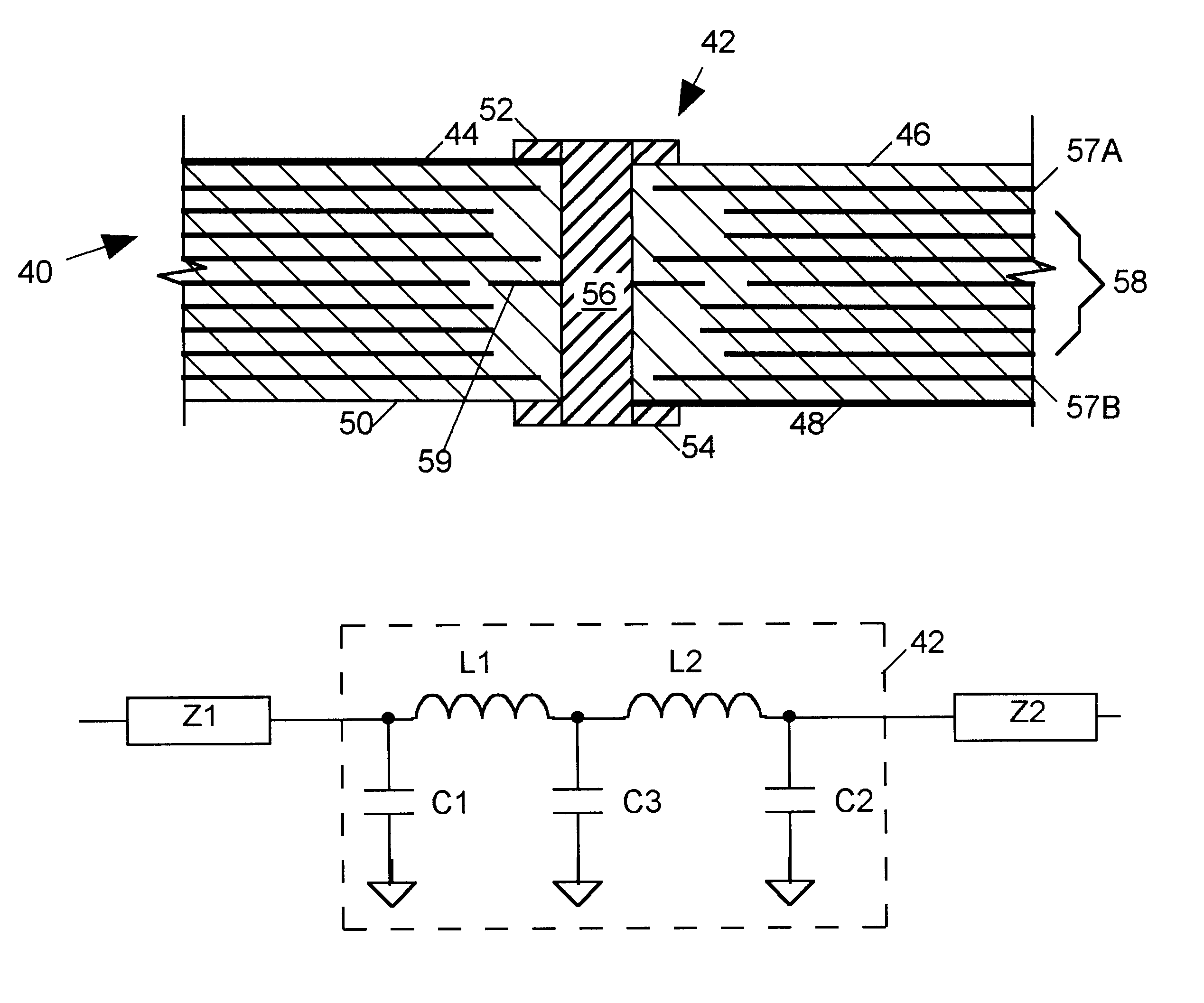
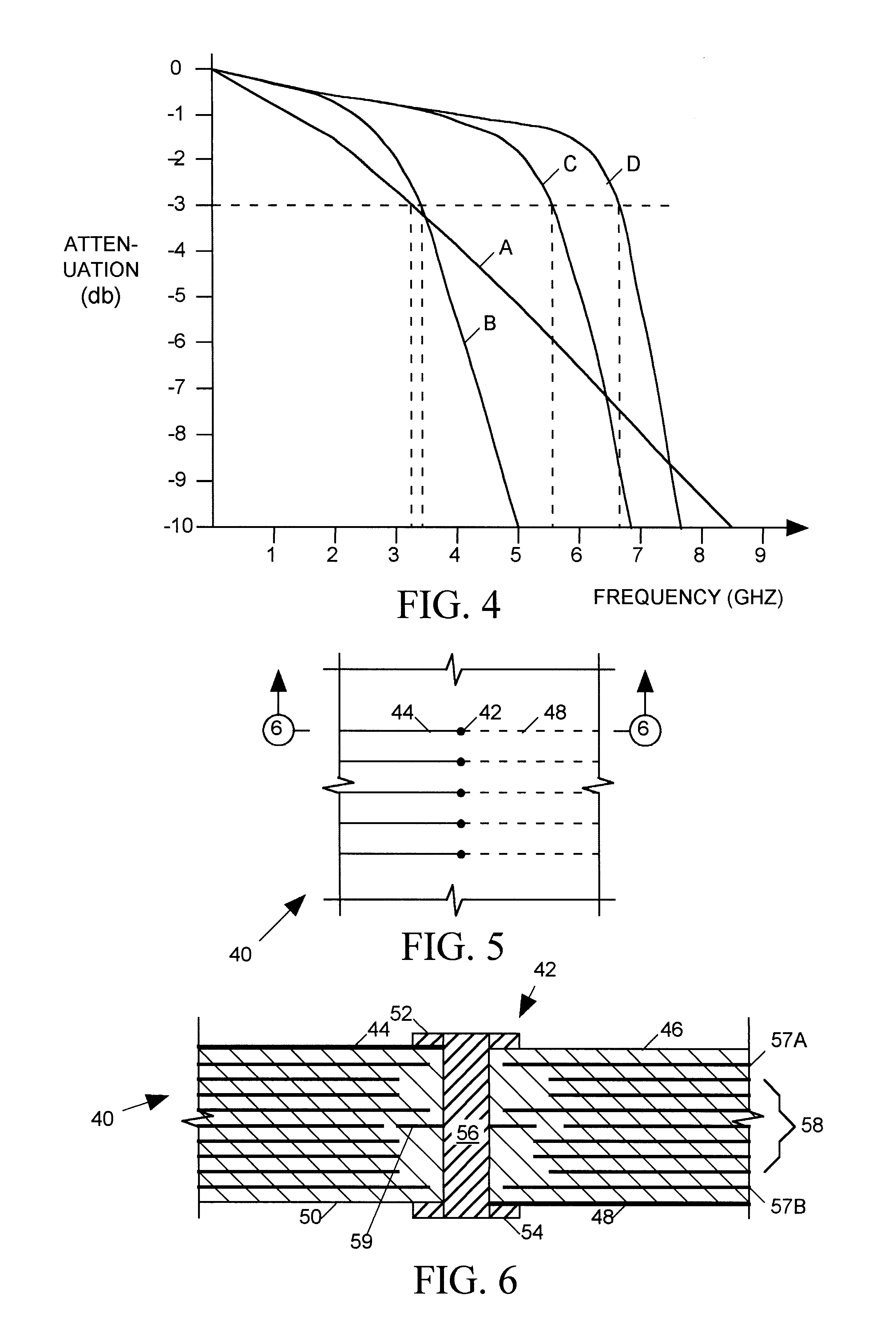
FIGS. 5 and 6 are plan and sectional elevation views of a portion of a multi-layer printed circuit board (PCB) 40 employing a conductive via 42 in accordance with the invention to link a microstrip conductor 44 formed on an upper surface 46 of PCB 40 to a microstrip conductor 48 formed on a lower surface 50 of the PCB. Via 42 includes an upper cap (annular ring 52) contacting conductor 34, a lower cap (annular ring 54) for contacting conductor 18 and a vertical conductor 56 extending between upper and lower annular rings 52 and 54. PCB 40 also includes power and ground planes 57A, 57B formed on substrate layers below upper surface 46 and above lower surface 50, and may also include additional embedded power and ground planes or signal planes 58 formed on other layers. Vertical conductor 56 passes though holes in power signal planes 57A, 57B and 58 that are sufficiently large to prevent conductor 56 from contacting planes 57A, 57B and 58.

In accordance with the invention a capacitor i...


PUM


Abstract

A printed circuit board (PCB) via, providing a conductor extending vertically between microstrip or stripline conductors formed on separate layers of a PCB, includes a conductive pad surrounding the conductor and embedded within the PCB between those PCB layers. The pad's shunt capacitance and the magnitudes of capacitances of other portions of the via are sized relative to the conductor's inherent inductance to optimize frequency response characteristics of the via.

Description

1. Field of the InventionThe present invention relates in general to a via for providing a signal path between conductors formed on separate layers of a printed circuit board, and in particular to a via that acts as a tuned filter to optimize characteristics of its frequency response.2. Description of Related ArtFIGS. 1 and 2 are plan and sectional elevation views of a portion of a prior art printed circuit board (PCB) employing a conductive via 12 to link a microstrip conductor 14 formed on an upper surface 16 of the PCB to a microstrip conductor 18 formed on a lower surface 20 of the PCB. Via 12 includes an upper cap (annular ring 22) contacting conductor 14, a lower cap (annular ring 24) contacting conductor 18 and a vertical conductor 26 extending between upper and lower annular rings 22 and 24. PCB 10 also includes embedded power and ground planes 28 formed on PCB substrate layers below upper surface 16 and above lower surface 20, and may also include additional embedded power,...

Claims


Application Information

Patent Timeline
Patent Type & Authority Patents(United States)
IPC IPC(8): H03H7/01H03H7/38H05K1/11H05K1/02H05K1/16H05K3/42H05K3/34H03H7/075
CPCH03H7/0115H03H7/38H05K1/0216H05K1/0251H05K1/116H05K1/162H03H7/1758H03H7/075H03H2001/0085H05K1/0231H05K1/0233H05K1/113H05K3/3421H05K3/429H05K2201/09263H05K2201/09454H05K2201/09672H05K2201/09727H05K2201/10689H05K1/02
Inventor HREISH, EMAD B.MILLER, CHARLES A.
Owner FORMFACTOR INC
Why Eureka
Try Eureka